Disk-like gettering unit, integrated circuit, encapsulated semiconductor device, and method for manufacturing the same
a technology of encapsulation and gettering material, which is applied in the direction of positive displacement liquid engine, optical radiation measurement, instruments, etc., can solve the problems of insufficient submission to act, inability to uniformly activate the gettering material, and inability to activate the inside gettering material
- Summary
- Abstract
- Description
- Claims
- Application Information
AI Technical Summary
Benefits of technology
Problems solved by technology
Method used
Image
Examples
first embodiment
[0116] (First Embodiment)
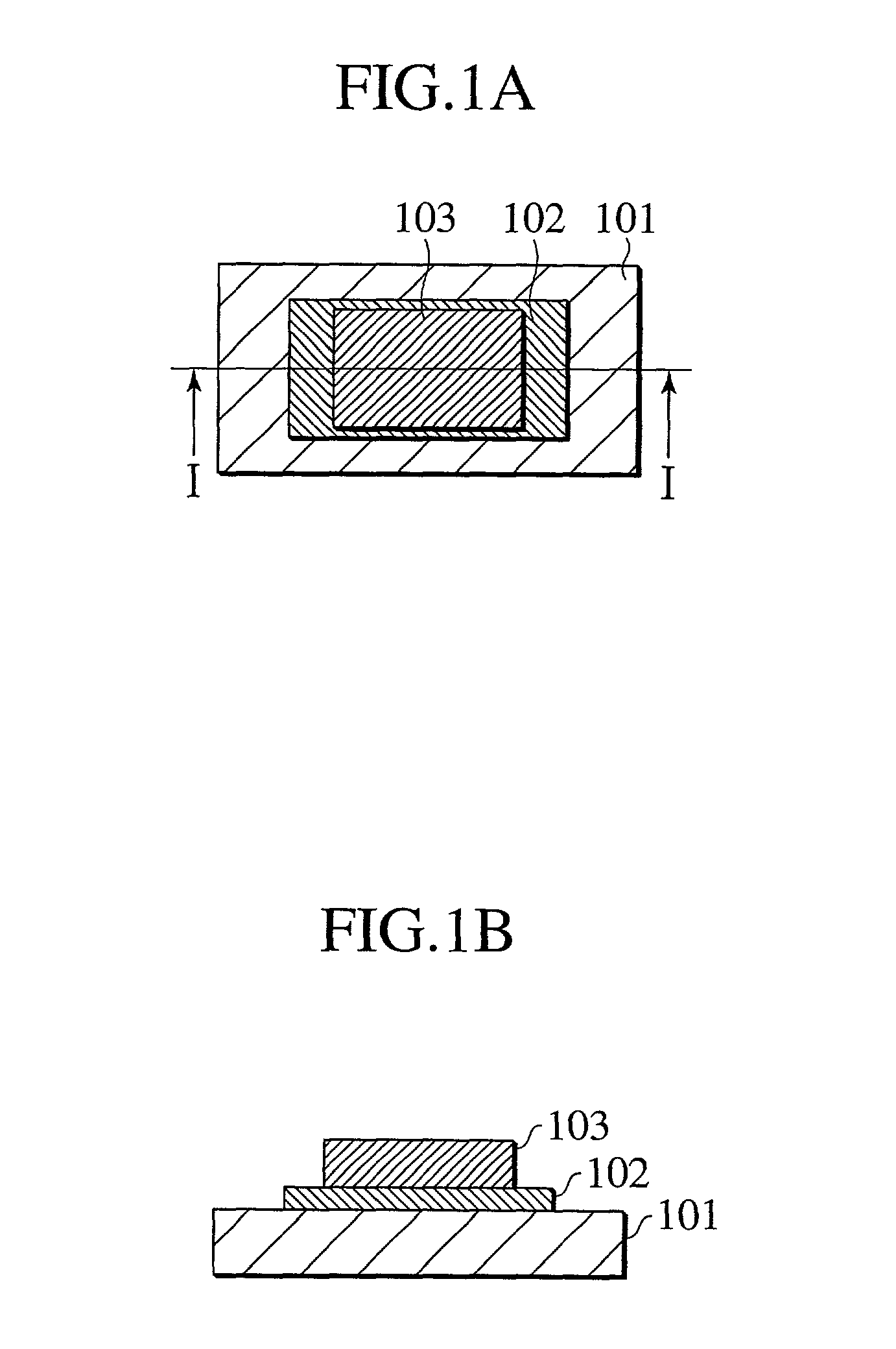
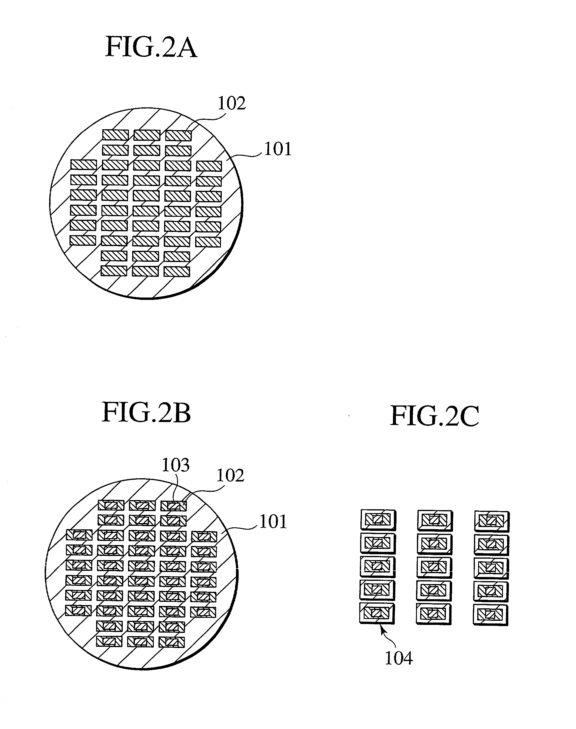
[0117] As shown in FIGS. 1A and 1B, a disk-like gettering unit according to the first embodiment encompasses a substrate 101, a thin film heater 102 disposed on the substrate 101, and a gettering layer 103 disposed selectively on the thin film heater 102. The gettering layer 103 serves as "a thin film gettering means" for adsorbing gaseous molecules in an enclosed space. The thin film heater 102 serves as "a thin film heating means" for heating two dimensionally the gettering means 103 so as to activate uniformly gettering action of the gettering means 103. The substrate 101 is "a supporting means" for supporting the gettering means 103 and heating means 102. The substrate 101 may be a semiconductor substrate, such as silicon (Si) substrate. It is also possible to use another substrates such as aluminum substrate or magnesia (MgO) substrate. And, the thin film heater 102 may be made of metallic film such as platinum (Pt) or chromium (Cr) film. The area of th...
second embodiment
[0129] (Second Embodiment)
[0130] As shown in FIG. 7A and 7B, a disk-like gettering unit according to the second embodiment encompasses a substrate 101, a thin film heater 102 disposed on the substrate 101, a buffer layer 203 disposed on the thin film heater 102, and a gettering layer 103 disposed on the buffer layer 203. The substrate 101 may be semiconductor substrate, such as silicon substrate. It is also possible to use another substrates such as aluminum substrate or magnesia substrate. The buffer layer 203 may made of insulating material which does not react with both of the gettering layer 103 and the thin film heater 102 at an elevated temperature for activation of the gettering layer 103. The buffer layer 203 may made of, for example, a silicon oxide (SiO.sub.2) film or aluminum (Al.sub.2O.sub.3) film. As shown in FIG. 7A, the buffer layer 203 covers wider than the area for the gettering layer 103. The buffer layer 203 does not cover two end terminals of the thin film heater...
third embodiment
[0137] (Third Embodiment)
[0138] As shown in FIGS. 10A and 10B, a disk-like gettering unit according to the third embodiment encompasses a substrate 101, a top thermally insulating layer 302 disposed on the top surface of the substrate 101, a bottom thermally insulating layer 302 disposed on the bottom surface of the substrate 101, a thin film heater 102 disposed on the top thermally insulating layer 302, and a gettering layer 103 disposed on the thin film heater 102. The substrate 101 may be semiconductor substrate, such as silicon substrate. It is also possible to use another substrates such as aluminum substrate or magnesia substrate.
[0139] Thermal conductivity of the top and bottom thermally insulating layers 302 is lower than that of the substrate 101. As an example of the top and bottom thermally insulating layers 302, the silicon oxide (SiO.sub.2) film can be employed. However, any low thermal conductivity materials other than the silicon oxide film can also be employed, as lo...
PUM
 Abstract
Description
Claims
Application Information
 - R&D
- Intellectual Property
- Life Sciences
- Materials
- Tech Scout
- Unparalleled Data Quality
- Higher Quality Content
- 60% Fewer Hallucinations
Browse by: Latest US Patents, China's latest patents, Technical Efficacy Thesaurus, Application Domain, Technology Topic, Popular Technical Reports.
© 2025 PatSnap. All rights reserved.Legal|Privacy policy|Modern Slavery Act Transparency Statement|Sitemap|About US| Contact US: help@patsnap.com


