Semiconductor physical quantity sensor
a technology of physical quantity and sensor, which is applied in the direction of turn-sensitive devices, instruments, force measurement, etc., can solve the problems of sensor not working normally, and the protrusion in the prior arts not working sufficiently
- Summary
- Abstract
- Description
- Claims
- Application Information
AI Technical Summary
Benefits of technology
Problems solved by technology
Method used
Image
Examples
first embodiment
[0035] (First Embodiment)
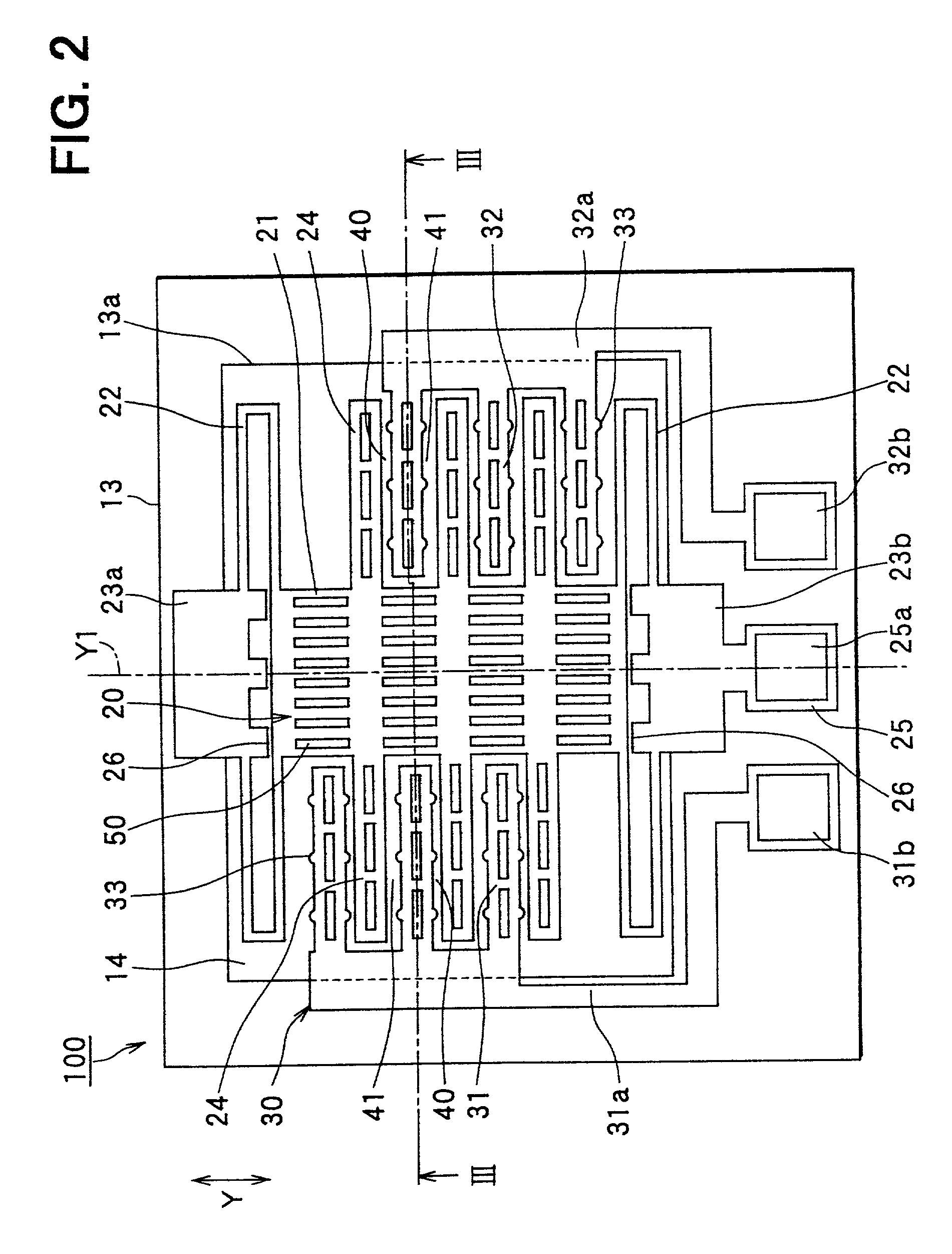
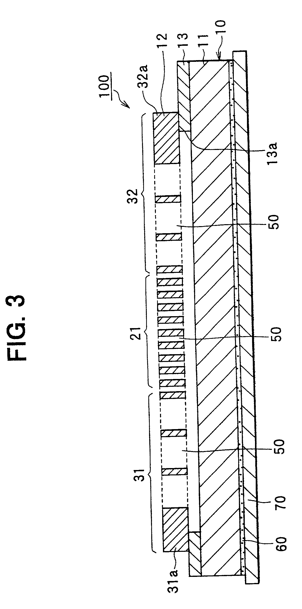
[0036] Referring to FIGS. 2 and 3, a semiconductor acceleration sensor 100 (which is simply referred to as a sensor 100 hereinafter) is formed as a rectangular sensor chip in a semiconductor substrate by a well-known micro-machined method. As shown in FIG. 3, the semiconductor substrate forming the sensor 100 is a SOI (Silicon On Insulator) substrate 10 which includes a first silicon substrate (supporting substrate) 11 as a first semiconductor layer, a second silicon substrate 12 as a second semiconductor layer, and an oxide layer 13 as a insulator layer interposed between the first silicon substrate 11 and the second silicon substrate 12.
[0037] A beam structure consisting of a movable portion 20 and fixed portion 30 is formed in the second silicon substrate 12. The movable portion 20 is separated from the fixed portion 30 by forming trenches 14. A part of the oxide layer 13 is removed under the beam structure by sacrificial layer etching to make a rectangul...
second embodiment
[0076] (Second Embodiment)
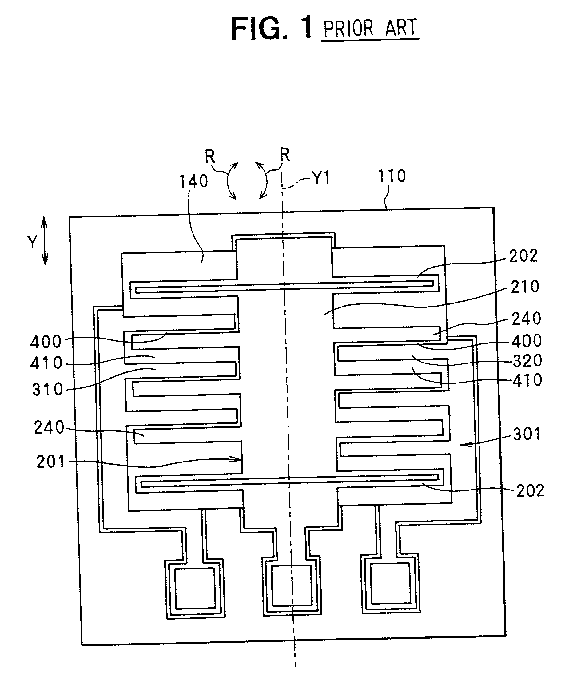
[0077] Miniaturization is required for a semiconductor physical quantity detection sensor such as the sensor described in Prior Art and the sensor 100 described above.
[0078] For this purpose, it is a useful way to shorten the suspension members 22 in its longitudinal direction in the sensor in FIG. 2. However, the length of the suspension portion is very important because it is main factor of spring modulus that contributes to a sensitivity of the sensor. Therefore, it is not so easy to shorten the length of the suspension members 22.
[0079] To solve the new problem described above, it is conceivable to connect several rectangle frame spring portions, each of which is formed with one pair of the suspension members 22, in series in a direction along the axis Y1. In the direction corresponding to the axis Y1, the number of folding times of each rectangle frame spring portion is only one. Therefore, if two rectangle frame spring portions are connected in series...
third embodiment
[0111] (Third Embodiment)
[0112] Referring to FIG. 12, a sensor 400 in this embodiment is the same as the sensor 300 in the second embodiment except that the protrusions 33 are not formed on the fixed electrodes 31 and 32 in the sensor 400.
[0113] A sensor 400 has a movable portion 20 and a fixed portion 30 on a first silicon substrate 11 (supporting substrate). The movable portion 20 has a weight portion 21 that is movable along a displacement direction Y due to an acceleration applied to the sensor, and comb-shaped movable electrodes 24 formed on both side surfaces of the weight portion 21 centering an axis Y1 in accordance with a displacement direction. The fixed portion 30 has fixed electrodes 31 and 32 each electrode members of which engaging with each of the movable electrodes 24 so as to oppose to the movable electrodes 24. This sensor 400 detects an acceleration applied to the sensor in the displacement direction Y based on a change of capacitance provided with the movable ele...
PUM
 Abstract
Description
Claims
Application Information
 - R&D
- Intellectual Property
- Life Sciences
- Materials
- Tech Scout
- Unparalleled Data Quality
- Higher Quality Content
- 60% Fewer Hallucinations
Browse by: Latest US Patents, China's latest patents, Technical Efficacy Thesaurus, Application Domain, Technology Topic, Popular Technical Reports.
© 2025 PatSnap. All rights reserved.Legal|Privacy policy|Modern Slavery Act Transparency Statement|Sitemap|About US| Contact US: help@patsnap.com


