Solder bump forming method and apparatus

a technology of soldering method and forming method, which is applied in the direction of soldering apparatus, manufacturing tools,auxillary welding devices, etc., can solve the problems of increased production cost, prolonged adjustment operation of positioning time, and inability to use methods that have not been widely used, so as to eliminate the limitation on the type of target substrate and be easily separated

Inactive Publication Date: 2001-08-02
VEECO INSTR
View PDF0 Cites 20 Cited by
  • Summary
  • Abstract
  • Description
  • Claims
  • Application Information

AI Technical Summary

Benefits of technology

[0026] The container 14 is composed, for example, of a heat resistance metal material such as aluminum which can withstand the heating temperature of the solder melt. The material for the container is not particularly limited to aluminum, however. The container 14 preferably has a heat insulated structure such as a double wall structure to maintain the temperature of the solder melt 12 constant. The heater 18 is provided to heat and melt a solid solder or to maintain the melted solder at a proper temperature. Therefore, it is preferred that a thermosensor is provided in the container 14 or the like and the heater 18 is controlled by this thermosensor. The heater 18 is not particularly limited, but preferably allows for easy temperature control. Examples of the heater 18 include electric resistance heaters such as a sheathed heater, induction heaters and other various heaters. The heater 18 can be embedded in a structural member of the container 14 to heat the solder melt 12 indirectly as shown in FIG. 1, but it may be provided within the container to be brought into direct contact with the solder melt 12, if needed. Alternatively, the heater 18 may be provided in the forming member 16 to heat the solder within the container 14 by heat conduction from the adjacent forming member.
[0050] It is preferred to preheat the substrate 24, particularly surface portions of the substrate 24 around the pads 22 on which solder bumps are formed. This prevents an abrupt temperature drop of the solder melt 12 when the solder melt 12 flows into chamber 26. The preheating may be achieved by preliminarily heating the substrate 24 from its back side or by providing a heater in the forming apparatus for heating the surface of the substrate, particularly the surface portions of the substrate around the pads. Conventional heaters can be used.

Problems solved by technology

However, these methods have not come into widespread use, because the methods require large scale apparatus and suffer from limitations on the bump density and type of solders that can be used.
However, this method of forming solder bumps requires a metal mask which is formed with minute holes in conformity with each terminal pattern of a chip, resulting in higher production costs.
Therefore, the time required for an adjustment operation for the positioning is prolonged, thereby reducing productivity.
Methods of physically applying an appropriate amount of a solder onto target pads are known, though these methods are not intended for solder bump formation.
Therefore, this method cannot be applied to solder bump formation.
This phenomenon is also observed in a solder wave operation and solder dip processes, which are also not readily adaptable to solder bump formation.

Method used


Image

  • Solder bump forming method and apparatus
  • Solder bump forming method and apparatus
  • Solder bump forming method and apparatus

Examples


Embodiment Construction

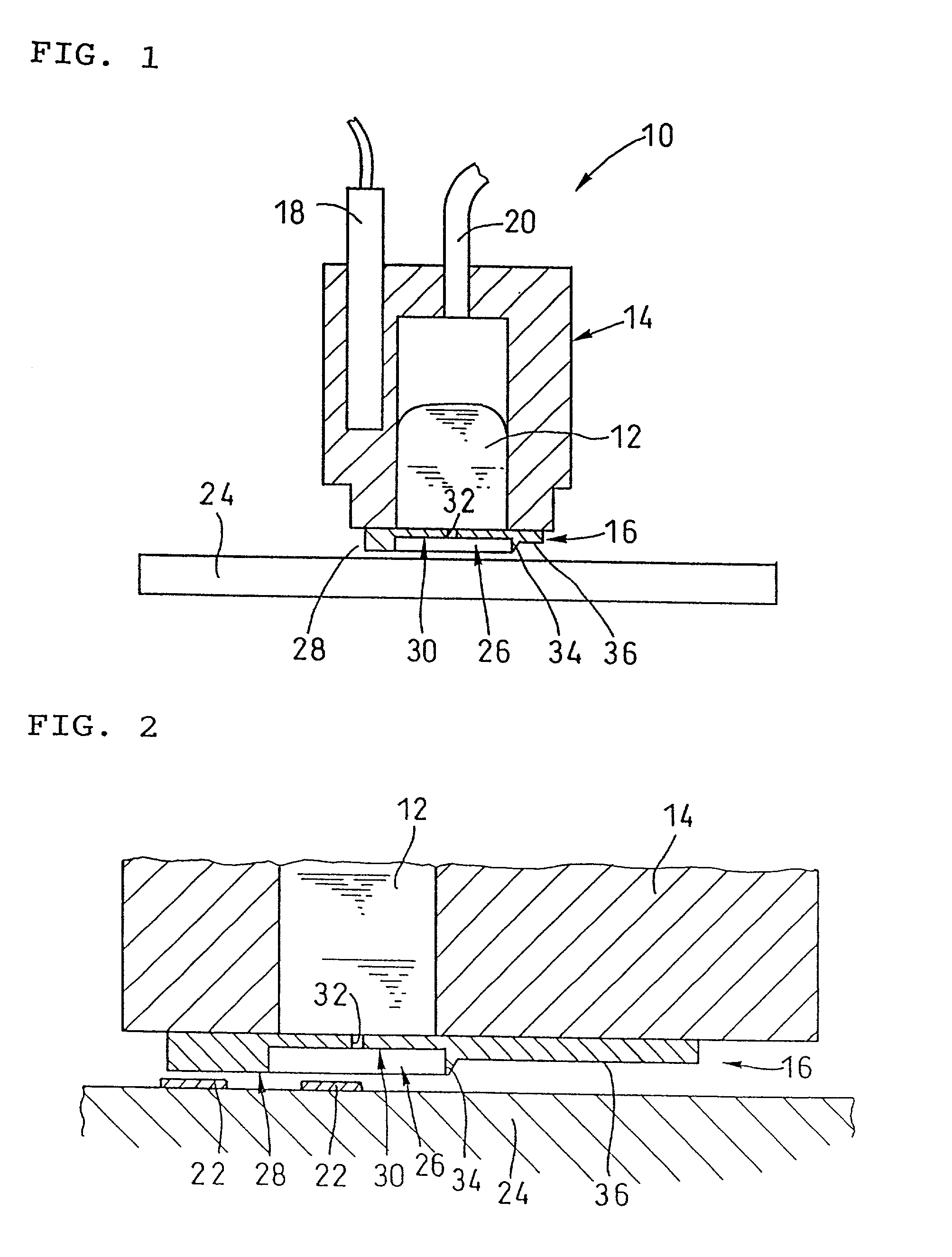
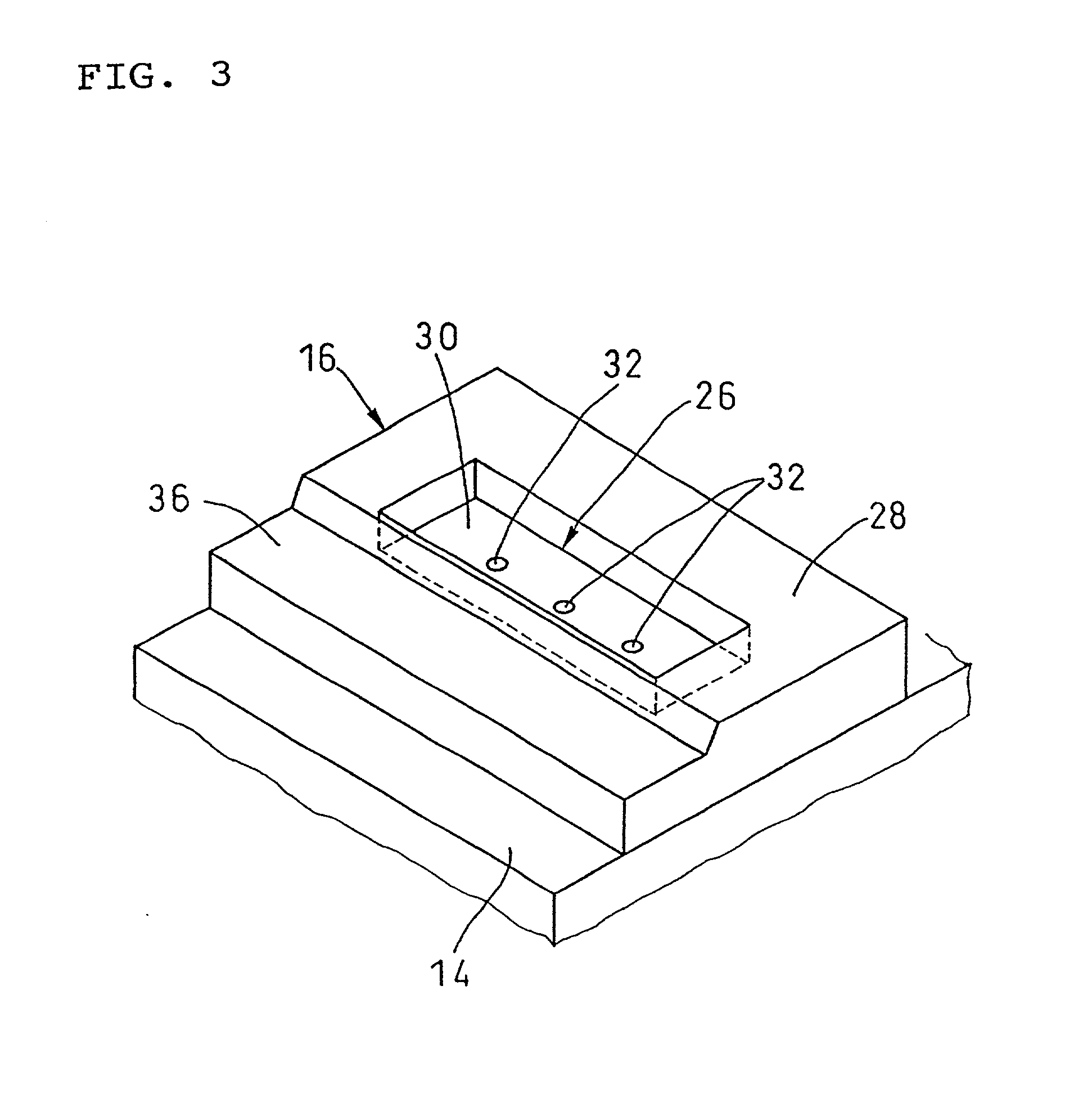
[0061] A eutectic solder was used, and a substrate was spaced 25 .mu.m from the flange portion and 55 .mu.m from the height regulator. The pressure of the gas was 150 gf / cm.sup.2. With this arrangement, bumps each having a height of 65 .mu.m were formed on 140-.mu.m diameter pads. The processing time was only about 5 to 10 seconds for each flip-chip pattern. This was possible because the formation of barrel-shaped solder melt fractions and the separation thereof from the chamber were carried out at a relatively high speed.

[0062] While there have been shown and described what are at present the preferred embodiments of the invention, it will be obvious to those skilled in the art that various changes and modifications may be made therein without departing from the scope of the invention as defined by the appended claims.

[0063] In the apparatus and method according to the present invention, the container-forming member assembly and the substrate having target pads thereon may be moved...


PUM

PropertyMeasurementUnit
Pressureaaaaaaaaaa
Shapeaaaaaaaaaa
Heightaaaaaaaaaa

Abstract

A bump forming apparatus comprises a container for retaining therein a solder melt, a solder forming member having a side wall portion and a ceiling portion which form, above a substrate's flat surface, a chamber for receiving therein the solder melt. The solder forming member also includes a height regulator portion provided on an exterior of the side wall portion and having a flat surface for restricting the height of the solder melt during formation. Heating means for heating the solder melt may also be provided. A hole in the solder forming portion allows solder melt to flow from the container to the chamber. Pressurizing means for pressurizing the solder melt in the container to thus expedite passage of solder melt into the chamber of the forming member may be used. Depressurization means for reducing the inside pressure of the container to cause the unused metal to return from the chamber into the container may also be used.

Description

[0001] The present invention relates to a method of and an apparatus for forming a solder bump. More particularly, the invention relates to a method of and an apparatus for forming a minute solder bump having an appropriate size on a substrate or a chip.[0002] The formation of extremely small solder bumps (balls) is a very important process in the production of many types of electronic devices, and is particularly important for flip-chip mounting of semiconductor chips on highly integrated cards and boards, chip carriers, etc. Therefore, various means for achieving such formation have been devised and utilized in the industry. Exemplary methods include a solder plating process and a solder powder bonding method. However, these methods have not come into widespread use, because the methods require large scale apparatus and suffer from limitations on the bump density and type of solders that can be used.[0003] One method that imposes a less strict limitation on the solder type and ens...

Claims


Application Information

Patent Timeline
IPC IPC(8): H01L21/60B23K3/06B23K35/14H01L21/48H05K3/34
CPCB23K3/0623B23K2201/40H01L21/4846H05K3/3457H05K2203/0126B23K2101/40
Inventor MAEDA, YOHJITSUKADA, YUTAKA
Owner VEECO INSTR
Why Eureka
Try Eureka