
Semiconductor memory device capable of operating at high speed, low power environment by optimizing latency of read command and write command depending on various operation modes

a memory device and memory technology, applied in the field can solve the problems of low power consumption, low efficiency, and low efficiency of semiconductor memory devices, and achieve the effect of reducing the number of flip-flops and reducing the area and current consumption

Active Publication Date: 2022-08-02
SK HYNIX INC
View PDF8 Cites 0 Cited by
  • Summary
  • Abstract
  • Description
  • Claims
  • Application Information

AI Technical Summary

Benefits of technology

[0010]According to embodiments described herein, the semiconductor memory device may operate at high speed in a low power environment by optimizing the latency of the read command and write command depending on various operation modes.
[0011]According to embodiments described herein, the semiconductor memory device may minimize the area and current consumption by reducing the number of flip-flops provided to control the latency of the read command and write command.

Problems solved by technology

However, since the SDR synchronous memory device is also insufficient to accommodate a system requiring high-speed operation, a double data rate (DDR) synchronous memory device, which processes two data items in one clock period, has been proposed.

Method used


Image

  • Semiconductor memory device capable of operating at high speed, low power environment by optimizing latency of read command and write command depending on various operation modes
  • Semiconductor memory device capable of operating at high speed, low power environment by optimizing latency of read command and write command depending on various operation modes
  • Semiconductor memory device capable of operating at high speed, low power environment by optimizing latency of read command and write command depending on various operation modes

Examples


first embodiment

[0079]FIG. 6 is a detailed circuit diagram illustrating the latency setting circuit 164 according to the present invention.

[0080]Referring to FIG. 6, the latency setting circuit 164 may include a write latency circuit 210 and a read latency circuit 230.

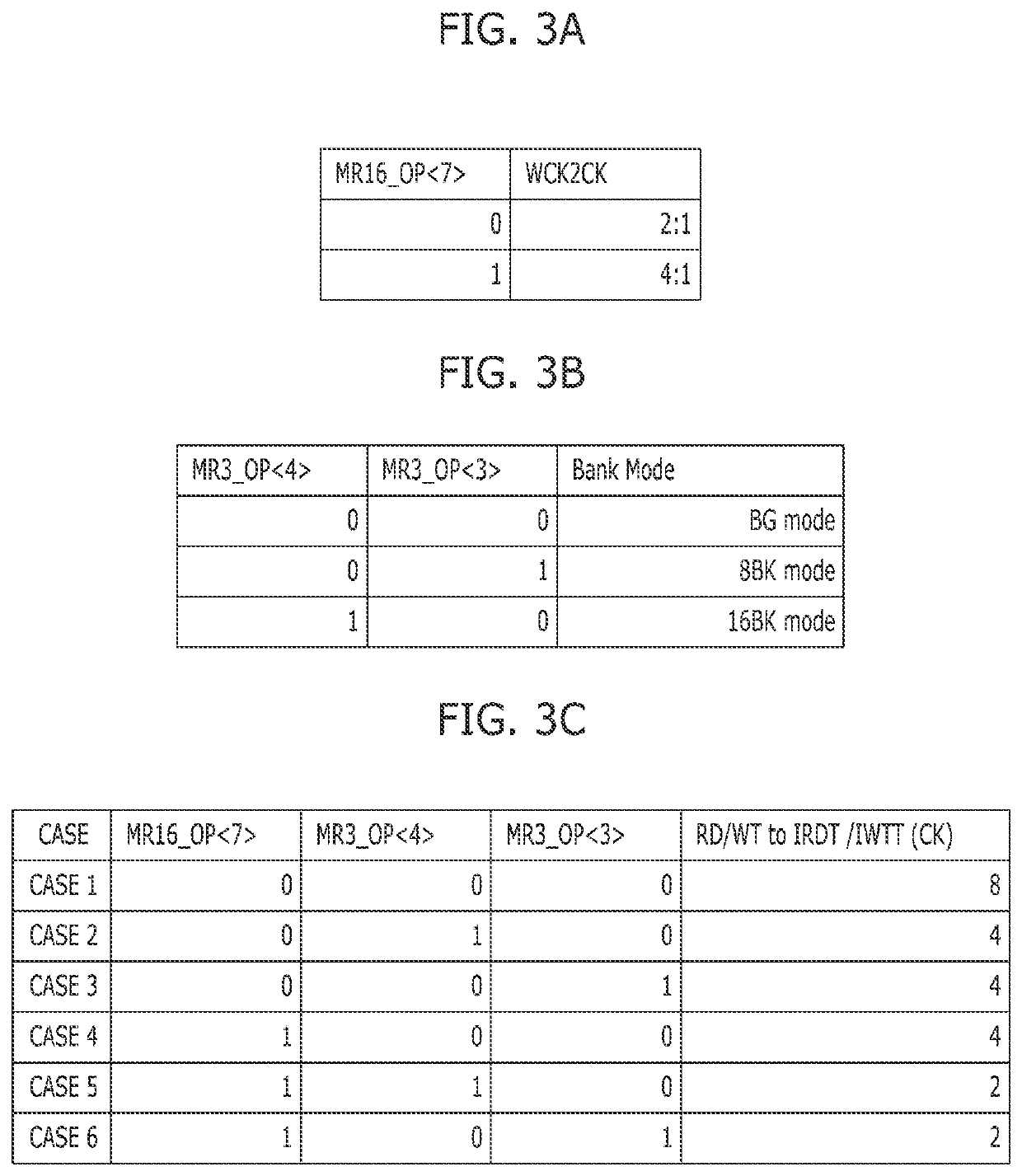
[0081]The write latency circuit 210 may include a preliminary latency circuit 212 and a main latency circuit 214. The preliminary latency circuit 212 may generate a preliminary write command WTT by delaying the write command WT by a first latency according to the write clock WT_CLK. In this case, the first latency is a delay time defined in the process from the input of the write command to the actual input of the write data and may correspond to ‘write latency WL+burst length BL / width (N) of one data item+1’. The main latency circuit 214 may set a second latency according to the first to third mode selection signals SEL1 to SEL3 and generate the internal write command IWTT by further delaying the preliminary write command WTT by the ...

second embodiment

[0086]FIG. 7 is a detailed circuit diagram illustrating the latency setting circuit 164 according to the present invention. FIG. 8 is a circuit diagram illustrating a control signal generating circuit 312 as illustrated in FIG. 7. FIG. 9 is a circuit diagram illustrating an interval defining circuit 314 as illustrated in FIG. 7. FIG. 10 is a circuit diagram illustrating a clock driver 316 as illustrated in FIG. 7.

[0087]Referring to FIG. 7, the latency setting circuit 164 may include a clock driving circuit 310, a write latency circuit 320, and a read latency circuit 330.

[0088]During a write operation, the clock driving circuit 310 may delay the write clock WT_CLK by the latency corresponding to the activated mode selection signal among the first to third mode selection signals SEL1 to SEL3 to thereby generate a write trigger signal WTCLK_BL32. During a read operation, the clock driving circuit 310 may delay the read clock RD_CLK by the latency corresponding to the activated mode sel...

third embodiment

[0117]Since two write commands WT are input in the bank group mode, the timing margin may not be sufficient as compared with that in the individual bank mode. A method for further securing a timing margin in the bank group mode is described below according to the present invention.

[0118]FIG. 13 is a detailed circuit diagram illustrating the latency setting circuit 164 according to a third embodiment of the present invention. FIG. 14 is a circuit diagram illustrating an interval defining circuit 514 as illustrated in FIG. 13. FIG. 15 is a circuit diagram illustrating a clock driver 516 as illustrated in FIG. 13.

[0119]Referring to FIG. 13, the latency setting circuit 164 may include a clock driving circuit 510, a write latency circuit 520, and a read latency circuit 530. The write latency circuit 520 and read latency circuit 530 of FIG. 13 are substantially the same in circuit configuration as the write latency circuit 320 and the read latency circuit 330 of FIG. 7, respectively.

[0120...


PUM


Abstract

A semiconductor memory device includes: a memory cell array including banks; a command / address buffer receiving a command / address based on a system clock; a data input / output circuit inputting / outputting data based on a data clock; a mode control circuit generating mode selection signals indicating different latencies according to a burst length signal and operation information on a first operation mode differentiated based on a ratio of the data clock to the system clock, and a second operation mode differentiated based on a bank mode; and a latency setting circuit setting a latency according to an activated one of the mode selection signals, generating an internal write command by delaying a write command at least by the set latency according to the system clock during a write operation, and generating an internal read command by delaying a read command by the set latency according to the system clock during a read operation.

Description

CROSS-REFERENCE TO RELATED APPLICATION[0001]The present application claims priority under 35 U.S.C. § 119 on Korean Patent Application No. 10-2020-0077046, filed on Jun. 24, 2020, which is herein incorporated by reference in its entirety.BACKGROUND1. Field[0002]Various embodiments described herein relate to a semiconductor design technology and, more particularly, to a synchronous semiconductor memory device.2. Description of the Related Art[0003]Semiconductor memory devices have been continuously improved to increase the degree of integration and to increase the operation speed thereof. To increase the operation speed, synchronous memory devices that can operate in synchronization with an external clock have been introduced. First proposed is a single data rate (SDR) synchronous memory device that inputs and outputs one data item over a period of a clock through one data pin in synchronization with a rising edge of the clock external to the memory device. However, since the SDR syn...

Claims


Application Information

Patent Timeline
Patent Type & Authority Patents(United States)
IPC IPC(8): G11C11/408G11C11/4076G11C11/4096
CPCG11C11/4076G11C11/4082G11C11/4087G11C11/4096G11C7/1072G11C11/409G11C5/063G06F13/1673G06F13/1689G06F3/0656G11C7/1045G11C7/222G11C2207/2272G11C7/1006G11C7/1051G11C7/1078G11C8/12
Inventor KIM, WOONGRAE
Owner SK HYNIX INC
Learn More