
Hybrid tandem solar cell

a solar cell and tandem technology, applied in the field of tandem solar cells, can solve the problems of low thermal robustness, inability to regularly solder cells for interconnection, and inability to process the top cell in case of a 2-terminal tandem structure, etc., to achieve improved thermal robustness of the bottom solar cell, reduce production costs, and improve thermal robustness

Active Publication Date: 2021-10-19
NEDERLANDSE ORG VOOR TOEGEPAST NATUURWETENSCHAPPELIJK ONDERZOEK TNO
View PDF6 Cites 0 Cited by
  • Summary
  • Abstract
  • Description
  • Claims
  • Application Information

AI Technical Summary

Benefits of technology

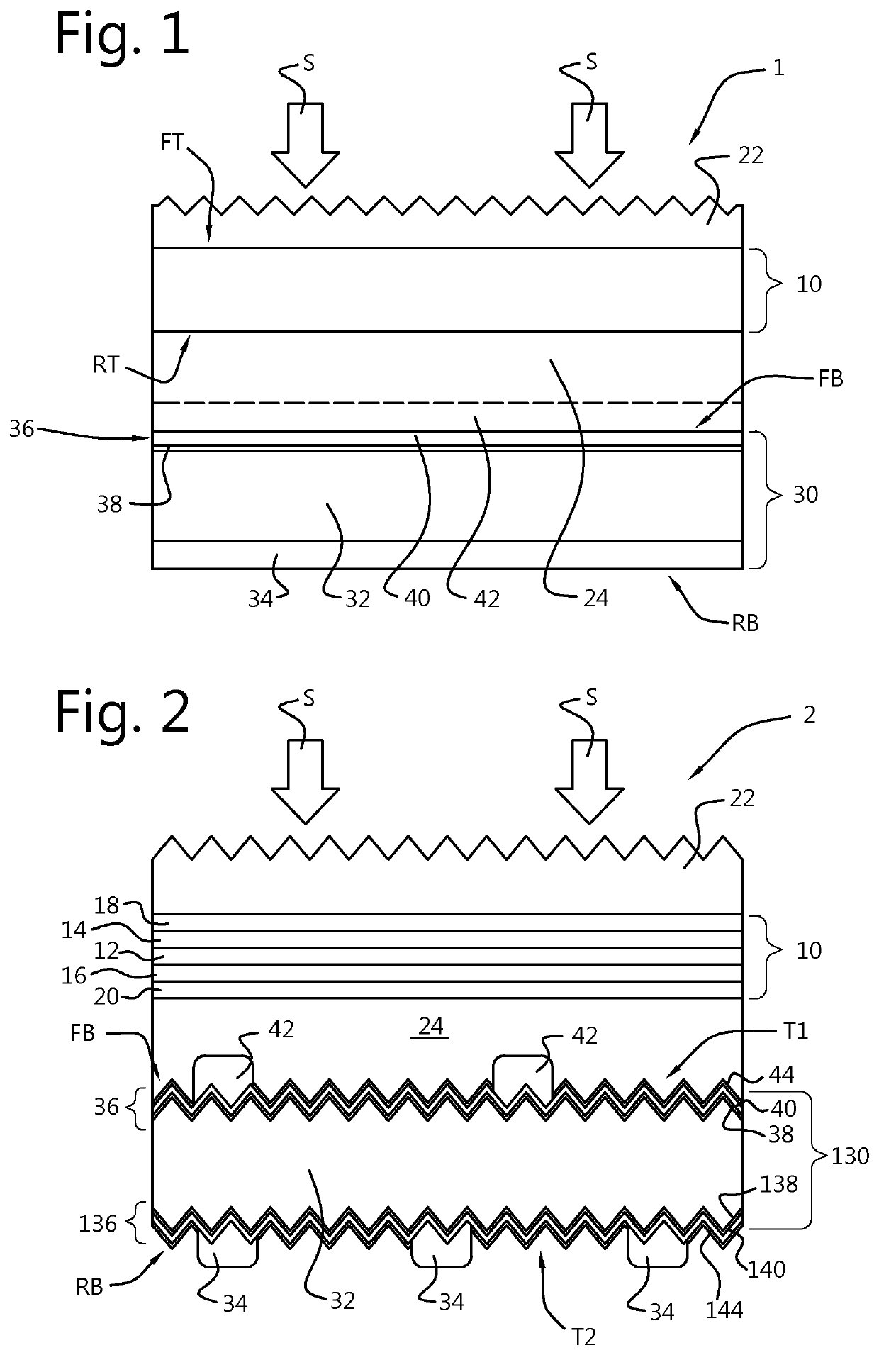
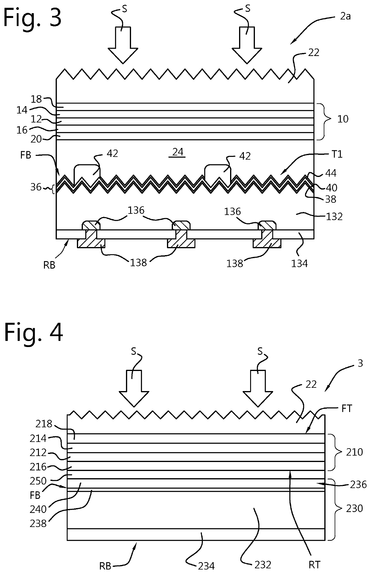
[0008]Advantageously, since the materials in the passivating layer stack can be chosen to be thermally stable structures compared to the amorphous heterojunction layers of the prior art, the invention provides an improved thermal robustness of the bottom solar cell, and a relatively lower production cost than for an amorphous silicon heterojunction cell as bottom solar cell in a tandem solar cell. Such high thermal robustness can allow to use manufacturing processes with relatively high temperature such as standard fire-through metallization, etc.
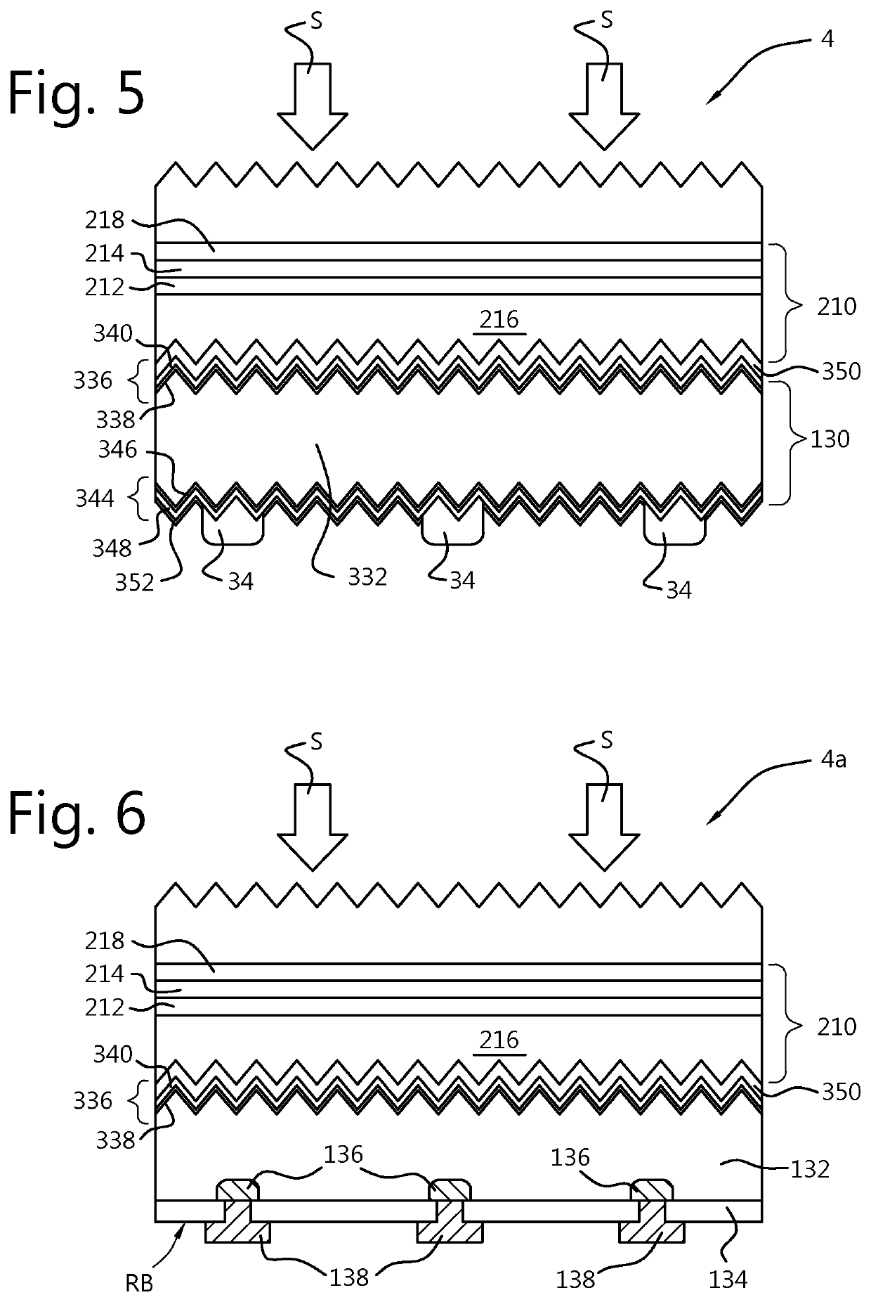
[0009]Also, to use a passivating layer stack with a combination of a thin passivating dielectric such as a tunnel oxide and a secondary layer can provide a comparatively low recombination rate of charge carriers which results in higher Voc and FF values, and higher performance of the tandem solar cell. This is particularly the case when the secondary layer provides for selective carrier extraction (also described as selective carrier collection) from the silicon substrate, in which case the passivating layer stack is known as a passivated contact or passivating contact. Enhancement of the tandem solar cell is also particularly the case when the secondary layer is an intrinsic (not intentionally doped, at most lightly doped) polysilicon layer, which does not result in a passivating contact but provides excellent passivation.
[0010]Moreover, the prior art application of a TCO electrode to compensate for low lateral conductance in the amorphous heterojunction can be omitted, as the selective carrier extracting material of the secondary layer, such as highly doped polysilicon of a thickness of at least several tens of nm's, can provide lateral conductance.
[0012]Thin dielectrics that yield good performance are e.g., silicon oxide (e.g. silicon dioxide) and silicon oxynitrides. Other possible thin dielectrics are for example aluminium oxide or hafnium oxide. A typical silicon oxide or oxynitride thickness is between ˜0.5 and ˜5 nm, preferably ˜1-˜2 nm. An thin oxide thicker than about 1.5 nm can fulfill the required function of good passivation and a sufficient transmission of majority charge carriers, and a sufficiently low transmission of minority charge carriers, depending on process conditions such as thermal anneal processes that create e.g. pinholes in the thin oxide film.
[0016]According to an aspect, the invention provides the tandem solar cell as described above wherein the secondary layer comprises poly-silicon. Typically, a film of poly-silicon with a thickness in the range from ˜5 to ˜500 nm has relatively high absorption in the visible range of the spectrum, but is transparent in the infrared range, which allows to use poly-silicon as a front layer for the bottom solar cell of the tandem solar cell. Thus, integration in a tandem solar cell structure is a solution to obtain the highest performance from silicon solar cells with a polysilicon passivating front contact or a polysilicon passivating front layer stack which otherwise (i.e., as stand-alone, single junction, use) would have very poor performance. Also, in stand-alone use of crystalline silicon cells with a polysilicon passivating contact, the polysilicon passivating contact is applied only to the back side, and additional process steps are required to provide e.g. a high quality diffused junction on the front side and lithography is required to provide contacts with very small contact area on the front side, to obtain high performance. According to an aspect of the invention, favorably polysilicon can be applied to both front and rear side of the silicon wafer, and for example the front and rear side polysilicon can be doped with opposite polarities, by e.g., printing a boron dopant source on one side and implanting phosphorus dopants on the other side, followed by a thermal anneal, resulting in a simple and low-cost cell process sequence for the bottom cell and yet a high performance of the tandem cell and module.
[0018]The polysilicon thickness can be in a range from ˜5 to ˜500 nm, where ˜10-˜200 nm is more optimal. For so-called fire-through contacting, ˜100 nm or thicker is preferable in order to avoid damage to the thin dielectric from the contacting metal penetrating the polysilicon layer.

Problems solved by technology

These disadvantages are e.g.: i) the low lateral conductance of the amorphous silicon heterojunction, which necessitates the use of transparent conductive oxide (TCO) electrodes, which (unless costly materials such as hydrogen or tungsten doped InOx, indium oxide, are used) have large IR absorption; ii) the low thermal robustness of amorphous silicon passivation which means that the resulting cells cannot be regularly soldered for interconnection, and processing of the top cell in case of a 2-terminal tandem structure is also thermally limited; iii) the complex process and high cost necessary for producing an interdigitated back contact version of a cell with amorphous silicon heterojunctions.

Method used


Image

  • Hybrid tandem solar cell
  • Hybrid tandem solar cell
  • Hybrid tandem solar cell

Examples


Embodiment Construction

lass="d_n">[0048]According to the present invention, the tandem solar cell comprises a stack of a top solar cell (or top photovoltaic device) and bottom solar cell (or bottom photovoltaic device), in which the top solar cell is arranged on top of the bottom solar cell. The top solar cell and the bottom solar cell are stacked in a manner that the rear surface of the top solar cell is stacked on the front surface of bottom solar cell.

[0049]The front surface refers to the surface of the respective solar cell that during use is substantially facing a radiation source (the sun). The rear surface refers to the surface of the respective solar cell that during use of the solar cell, is turned away from the radiation source.

[0050]The band gaps of the top solar cell photovoltaic material and the bottom solar cell photovoltaic material are configured in such a manner that the top solar cell is substantially transparent for radiation with wavelengths which are to be absorbed by the bottom solar...


PUM

PropertyMeasurementUnit
thicknessaaaaaaaaaa
thicknessaaaaaaaaaa
thicknessaaaaaaaaaa

Abstract

A tandem solar cell includes a top solar cell and a bottom solar cell. The top solar cell and the bottom solar cell each have a respective front surface and a rear surface, with the respective front surfaces being adapted for facing a radiation source during use. The top solar cell is arranged with its rear surface overlying the front surface of the bottom solar cell. The top solar cell includes a photovoltaic absorber layer with a bandgap greater than that of crystalline silicon. The bottom solar cell includes a crystalline silicon substrate. On at least a portion of the front surface of the bottom solar cell a passivating layer stack is disposed which includes a thin dielectric film and a secondary layer of either selective carrier extracting material or polysilicon. The thin dielectric film is arranged between the silicon substrate and the secondary layer.

Description

FIELD OF THE INVENTION[0001]The present invention relates to a tandem solar cell. Moreover, the invention relates to a method for manufacturing such a tandem solar cell. Also, the invention relates to a solar panel comprising at least one such tandem solar cell.BACKGROUND ART[0002]Tandem solar cells are known consisting of a crystalline silicon bottom cell with amorphous silicon (a-Si) heterojunctions, and a higher bandgap top solar cell. While the bottom solar cell thanks to the a-Si heterojunctions provides high Voc, which is beneficial for tandem performance, this bottom solar cell design has several disadvantages. These disadvantages are e.g.: i) the low lateral conductance of the amorphous silicon heterojunction, which necessitates the use of transparent conductive oxide (TCO) electrodes, which (unless costly materials such as hydrogen or tungsten doped InOx, indium oxide, are used) have large IR absorption; ii) the low thermal robustness of amorphous silicon passivation which ...

Claims


Application Information

Patent Timeline
Patent Type & Authority Patents(United States)
IPC IPC(8): H01L31/0725H01L31/078H01L51/42H01L51/44H01L31/0224H01L27/30H01L31/0236H01L31/18H01L31/043
CPCH01L31/0725H01L27/302H01L31/02245H01L31/02366H01L31/022425H01L31/022441H01L31/022466H01L31/043H01L31/078H01L31/1868H01L31/1884H01L51/4213H01L51/445Y02E10/549Y02P70/50H10K30/57H10K30/10H10K30/83H10K85/50
Inventor GEERLIGS, LAMBERT JOHANWU, YUZHANG, DONGVAN ROOSMALEN, JOHANNES ADRIANUS MARIALUXEMBOURG, STEFAN LIBERTUSVEENSTRA, SIEGFRIED CHRISTIAAN
Owner NEDERLANDSE ORG VOOR TOEGEPAST NATUURWETENSCHAPPELIJK ONDERZOEK TNO
Learn More