GaN transistor with integrated drain voltage sense for fast overcurrent and short circuit protection

a gallium nitride and transistor technology, applied in the direction of resistors, emergency protection arrangements for automatic disconnection, electrical equipment, etc., can solve the problems of igbts (insulated gate bipolar transistors) being too slow for protecting faster gan power devices, slow ocp options, and not meeting the requirements of gan devices

Active Publication Date: 2021-08-03
GAN SYST
View PDF8 Cites 2 Cited by
  • Summary
  • Abstract
  • Description
  • Claims
  • Application Information

AI Technical Summary

Benefits of technology

[0009]The present invention seeks to provide integrated overcurrent and short circuit protection for devices and systems comprising GaN transistors, which mitigates or circumvents one or more limitations of known solutions, or at least provides an alternative.
[0020]In some embodiments, the fast turn-off may be implemented as a one stage turn-off. For example, the FLT signal is passed through an inverter and an AND gate an input to the gate driver of driver circuit. When the FLT signal reaches the predetermined level, e.g. 5V, for overcurrent protection, the gate driver rapidly and fully turns-off the gate of the GaN transistor switch SW_MAIN. Rapid, single stage hard turn-off can be used bring the gate to source voltage Vgs to several volts below the threshold voltage, e.g. to −3V, within less than 100 ns, and preferably within 40 ns. Single stage hard turn-off may offer a solution for rapid overcurrent and short circuit protection for low current, high voltage GaN transistors comprising an integrated drain voltage sense circuit.
[0022]Two stage turn-off is beneficial for applications of devices and systems comprising high voltage / high current GaN power transistors and for lower power, low voltage GaN transistors. For example, rapid hard turn-off of a large gate width lateral GaN power transistor carrying a significant overcurrent may cause large transients and oscillations, which could potentially lead to device failure. Multi-stage turn-off, comprising fast soft turn-off followed by controlled delayed of full turn-off, assists in mitigating these issues and maintaining safe operating conditions.

Problems solved by technology

Industry standard OCP options for IGBTs (Insulated Gate Bipolar Transistors) are typically too slow for protecting faster GaN power devices.
For example, the following methods for overcurrent protection are known: De-saturation detection: widely used for SiC IGBTs; however, this method of OCP is slow and may not meet the requirements for GaN devices.
Current sense resistor: a low-cost solution, but it adds parasitic inductance, which adversely affects switching performance.
Di / dt detection by voltage sensing across a common source inductance: this approach is suitable for an IGBT module but not appropriate for GaN switches in which it is desirable to minimize source inductance.

Method used


Image

  • GaN transistor with integrated drain voltage sense for fast overcurrent and short circuit protection
  • GaN transistor with integrated drain voltage sense for fast overcurrent and short circuit protection
  • GaN transistor with integrated drain voltage sense for fast overcurrent and short circuit protection

Examples


example

OCP for Large Area, High Voltage / High Current GaN E-HEMT with Integrated Drain Voltage Sense

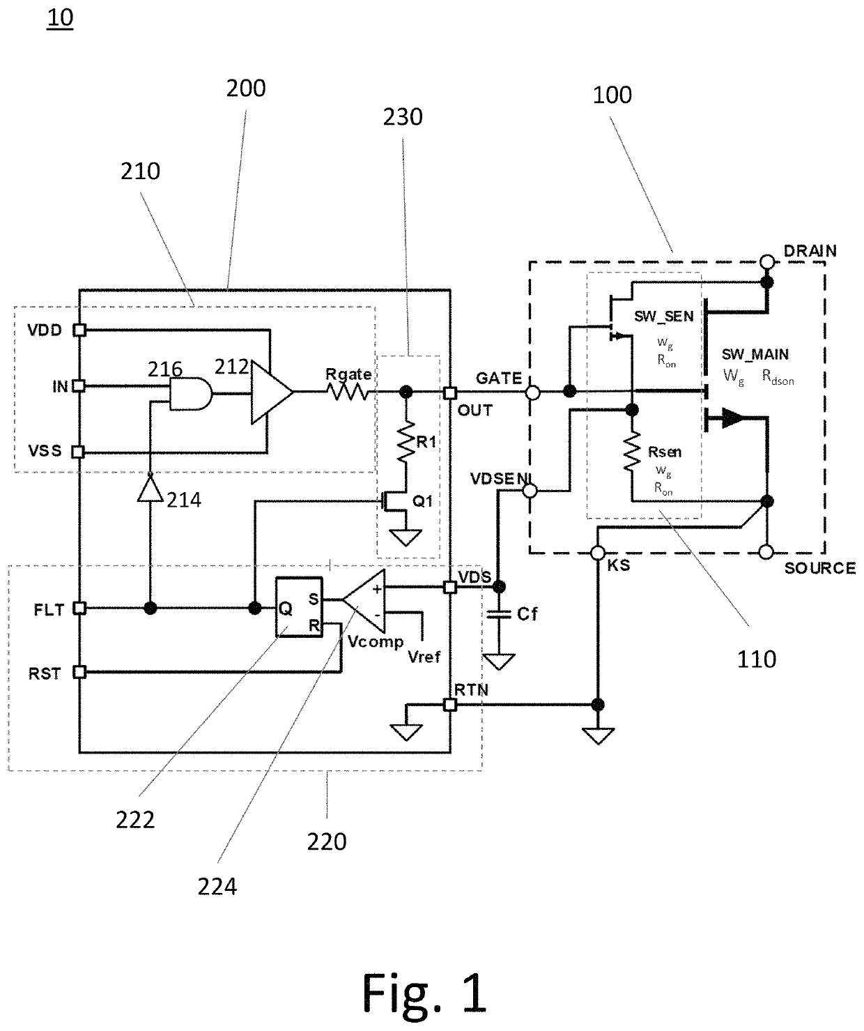
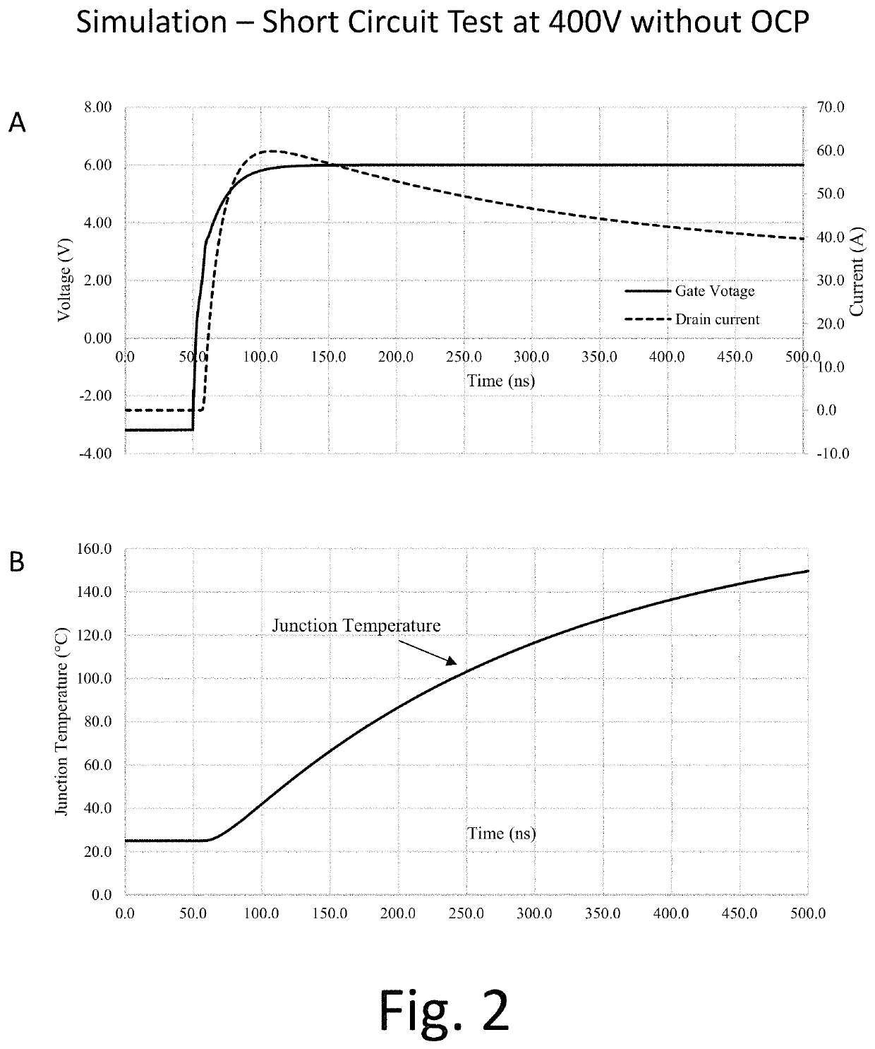
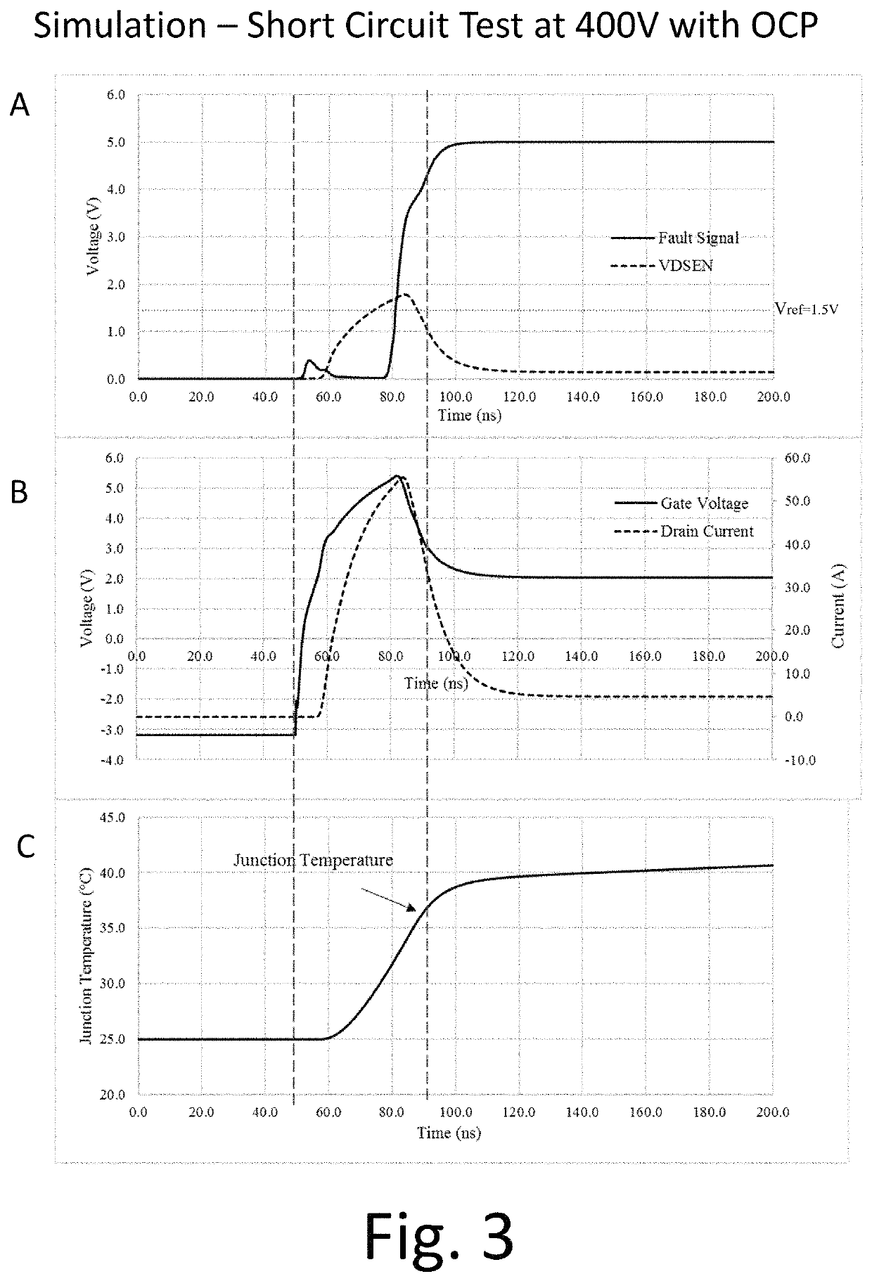
[0039]The operation of the system illustrated in FIG. 1 will be described in more detail, by way of example, with reference to simulation results based on a lateral GaN power switch SW_MAIN, which comprises a large area, large gate width lateral GaN E-HEMT. Simulation results for a GaN E-HEMT in the form of a 650V / 50 mΩ device which has a gate width Wg=300 mm and a drain-source on-resistance, Rdson, of 50 mΩ are shown in FIGS. 2 to 4.

[0040]It is desirable that the drain voltage sensing circuit 110 takes up minimal space on the GaN die 100 and that SW_SEN and Rsen are small enough so that they carry a small proportion of the current carried by the GaN switch SW_MAIN, for example, a current of only tens of mA. On the other hand, since Rsen is part of the SW_SEN gate drive loop that controls or limits the switching speed of SW_SEN, the gate widths wg of SW_SEN and Rsen should be large enough pro...


PUM

PropertyMeasurementUnit
on-resistancesaaaaaaaaaa
survival timeaaaaaaaaaa
threshold voltageaaaaaaaaaa

Abstract

A GaN power switching device comprises a GaN transistor switch SW_MAIN has an integrated drain voltage sense circuit, which comprises GaN sense transistor SW_SEN and GaN sense resistor RSEN, which at turn-on form a resistive divider for sensing the drain voltage of SW_MAIN to provide a drain voltage sense output VDSEN. Fault detection logic circuitry of a driver circuit generates a fault signal FLT when VDSEN reaches or exceeds a reference voltage Vref, which triggers fast turn-off of the gate of SW_MAIN, e.g. within less than 100 ns of an overcurrent or short circuit condition. During turn-off, RSEN resets VDSEN to zero. For two stage turn-off, the driver circuit further comprises fast soft turn-off circuitry which is triggered first by the fault signal to pull-down the gate voltage to the threshold voltage, followed by a delay before full turn-off of the gate of SW_MAIN by the gate driver.

Description

CROSS-REFERENCE TO RELATED APPLICATION(S)[0001]N / ATECHNICAL FIELD[0002]The present invention relates to overcurrent and short circuit protection for devices and systems comprising gallium nitride (GaN) transistors, including GaN power switches, such as, high current / high voltage GaN High Electron Mobility Transistors (GaN HEMTs).BACKGROUND ART[0003]Fast wide bandgap semiconductor power devices, such as Silicon Carbide (SiC) or Gallium Nitride (GaN) transistors require fast short circuit and overcurrent protection (OCP). Industry standard OCP options for IGBTs (Insulated Gate Bipolar Transistors) are typically too slow for protecting faster GaN power devices. The thermal mass of a lateral GaN HEMT is small; e.g., during a short circuit or overcurrent, a lateral GaN HEMT may heat up very quickly and have a survival time of only 300 ns to 500 ns. An IGBT is typically more robust and can survive a few microseconds.[0004]For example, the following methods for overcurrent protection are k...

Claims


Application Information

Patent Timeline
Patent Type & Authority Patents(United States)
IPC IPC(8): H02H3/00H03K17/081H01L29/20H01L29/423H01L29/778H03K17/082H03K17/16H01L25/18H01L27/06H01L49/02
CPCH03K17/08104H01L29/2003H01L29/42316H01L29/7787H03K17/0822H03K17/163H01L25/18H01L27/0605H01L27/0629H01L28/20
Inventor CHEN, DISPAZIANI, LARRY
Owner GAN SYST
Why Eureka
Try Eureka