
Snapback electrostatic discharge protection for electronic circuits

a technology of electrostatic discharge protection and electronic circuit, which is applied in the direction of diodes, semiconductor devices, transistors, etc., can solve the problems of limiting performance, snapback operation cannot be validated in conventional cad environments, and esd causes more than one-third of in-field failures in the semiconductor industry

Active Publication Date: 2021-07-06
WESTERN DIGITAL TECH INC
View PDF19 Cites 6 Cited by
  • Summary
  • Abstract
  • Description
  • Claims
  • Application Information

AI Technical Summary

Benefits of technology

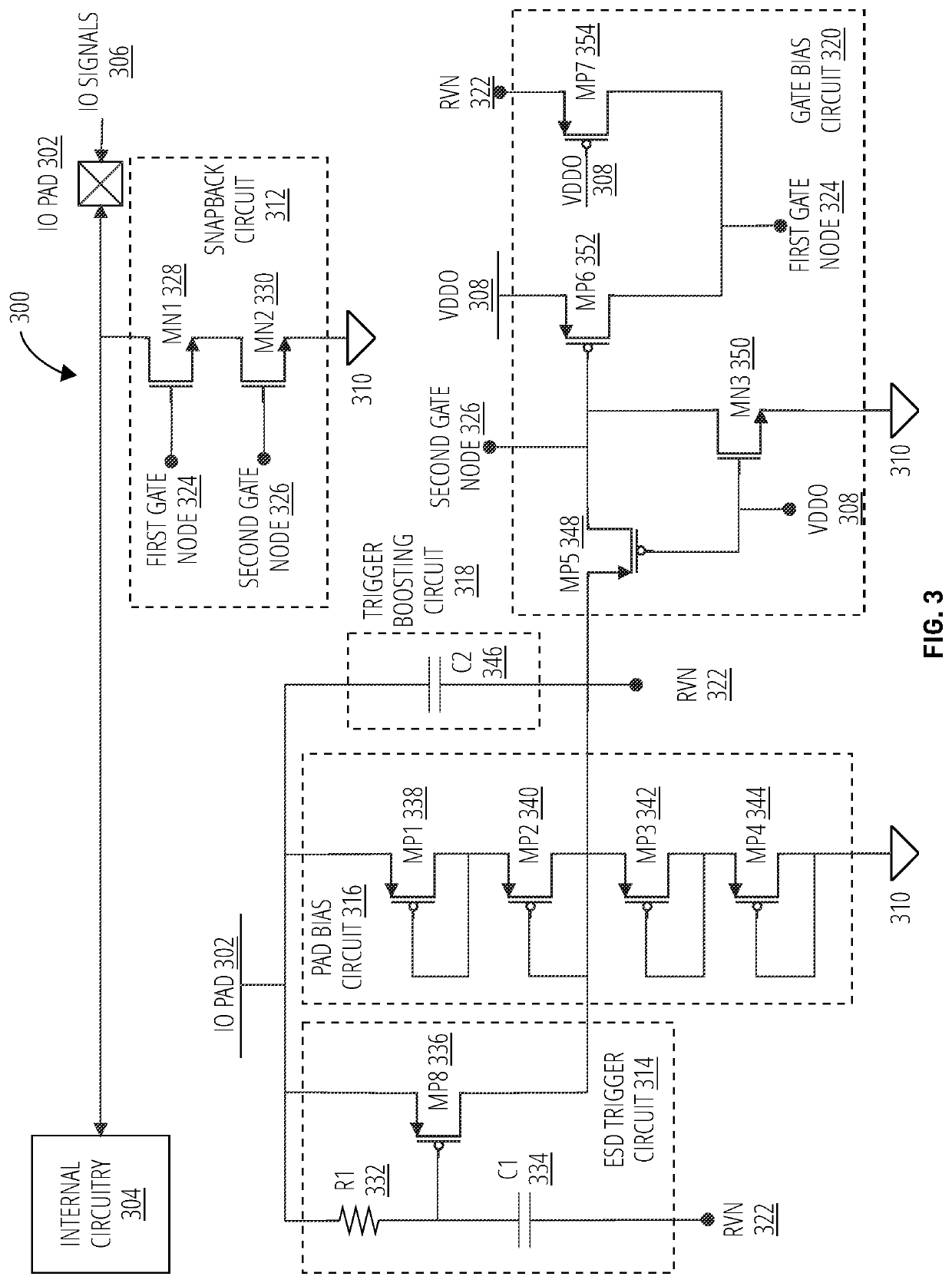
This patent describes an electrostatic discharge (ESD) protection circuit for memory dies. The circuit includes an input / output pad, a ground source, two NMOS transistors, a trigger circuit, a pad bias circuit, and a gate bias circuit. The trigger circuit detects an ESD event at the input / output pad and the fail-safe protection circuit manages a voltage level for the reference voltage node to prevent damage to the circuit. The gate bias circuit dynamically controls the voltage levels for the first and second gate nodes. The circuit can be used in a control bus of a memory die to protect against ESD events.

Problems solved by technology

ESD causes more than one-third of the in-field failures in the semiconductor industry.
The shrinking size of semiconductor chips, thin gate oxides, multiple power supplies, chip complexity, and high-speed circuit operation contribute significantly to ESD sensitivity and risk.
A reasonable protection of up to 2 kV may require a large device area and thus a large cost, as well as higher parasitic capacitance, which may limit performance.
Snapback operation cannot be validated in conventional CAD environments due to lack of availability of design models under ESD conditions.
Thus, there is a high risk that design flaws and / or deficiencies may not be identified until after wafers and dies are manufactured.
Snapback based ESD (SESD) protection circuits have been proposed, but these SESD protection circuits may not provide effective protection in advanced technologies like as 28 nm, 16 nm etc effective beta of BJT device is quite small.
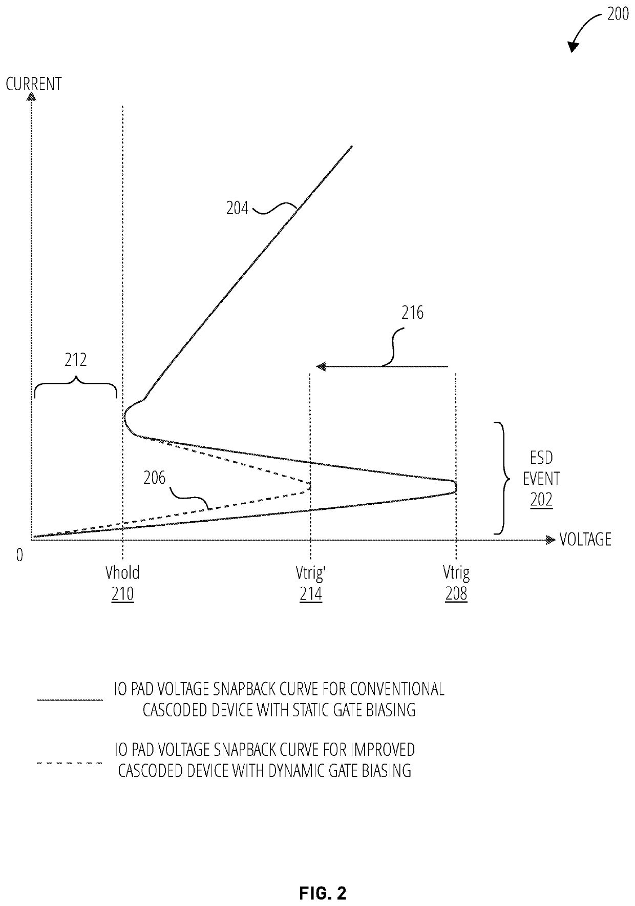
The triggering voltage of snapback devices may be unfavorably high, resulting in large inherent voltage buildup before an SESD circuit responds, which may increase susceptibility to circuit component failure.
Cascoding of the components for higher voltage operation support in the snapback circuit may further increase the triggering voltage needed, resulting an even higher failure risk.

Method used


Image

  • Snapback electrostatic discharge protection for electronic circuits
  • Snapback electrostatic discharge protection for electronic circuits
  • Snapback electrostatic discharge protection for electronic circuits

Examples


Embodiment Construction

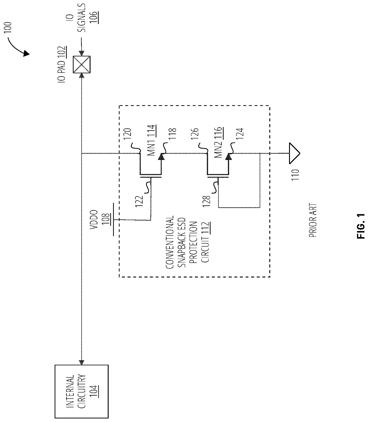
[0016]In conventional snapback protection circuits, the gate of one or more snapback devices is tied to ground, or effectively 0 V. Thus, the device channel doesn't take part in current flow as the channel is never turned on with the gate tied low. An improved ESD protective architecture is presented herein, which triggers the gate of one or more snapback devices to supplement ESD current discharge. Embodiments presented herein may also provide overvoltage tolerance (OVT) without increasing the triggering voltage. For example, 3.3V pad protection may be provided on devices using 1.8V without increasing the triggering voltage. In certain embodiments, fail-safe protection may also be provided without increasing the triggering voltage.

[0017]The solution disclosed herein may provide improvement regarding the challenges previously discussed. As the gate of the SESD device is triggered during an ESD event, instead of being tied to ground, the gate may be included in the ground path for th...


PUM


Abstract

Snapback ESD protection circuits that include an Input / Output pad, a ground source, a first and a second NMOS transistor, and trigger circuit, pad bias circuit, and gate bias circuit. The first transistor drain connects to the pad. The second transistor drain connects to the first transistor source. The second transistor source connects to ground. The trigger circuit connects to the pad and a reference voltage to detect an ESD event at the pad. The pad bias circuit connects to the pad, the trigger circuit, ground, and the reference voltage to manage a voltage level for the reference voltage. The gate bias circuit connects to the reference voltage, a supply voltage, ground, and the gates of the first and second transistor to dynamically control the voltage of each gate of the first and a second NMOS transistor.

Description

BACKGROUND[0001]Electrostatic discharge (ESD) is the sudden flow of electricity between two electrically charged objects caused by contact, an electrical short, or dielectric breakdown. ESD causes more than one-third of the in-field failures in the semiconductor industry. The shrinking size of semiconductor chips, thin gate oxides, multiple power supplies, chip complexity, and high-speed circuit operation contribute significantly to ESD sensitivity and risk.[0002]ESD protection circuits may be added on signal lines near locations where the lines may be exposed to external circuits, components, and / or effects such as ESD. Because ESD protection circuits are single-purpose circuits designed to protect other circuits from an ESD event, manufacturers desire to make ESD protection circuits as small as possible and that they to consume little or no power. “ESD event” refers to a sudden discharge of charge from a charge carrier into an electrical circuit.[0003]It is advantageous to have th...

Claims


Application Information

Patent Timeline
Patent Type & Authority Patents(United States)
IPC IPC(8): H02H9/04H01L27/02
CPCH02H9/046H01L27/0266H01L27/0255
Inventor MATHUR, SHIV HARITGUPTA, NITIN
Owner WESTERN DIGITAL TECH INC
Learn More