Memory array organization and related test method particularly well suited for integrated circuits having write-once memory arrays
- Summary
- Abstract
- Description
- Claims
- Application Information
AI Technical Summary
Problems solved by technology
Method used
Image
Examples
Embodiment Construction
)
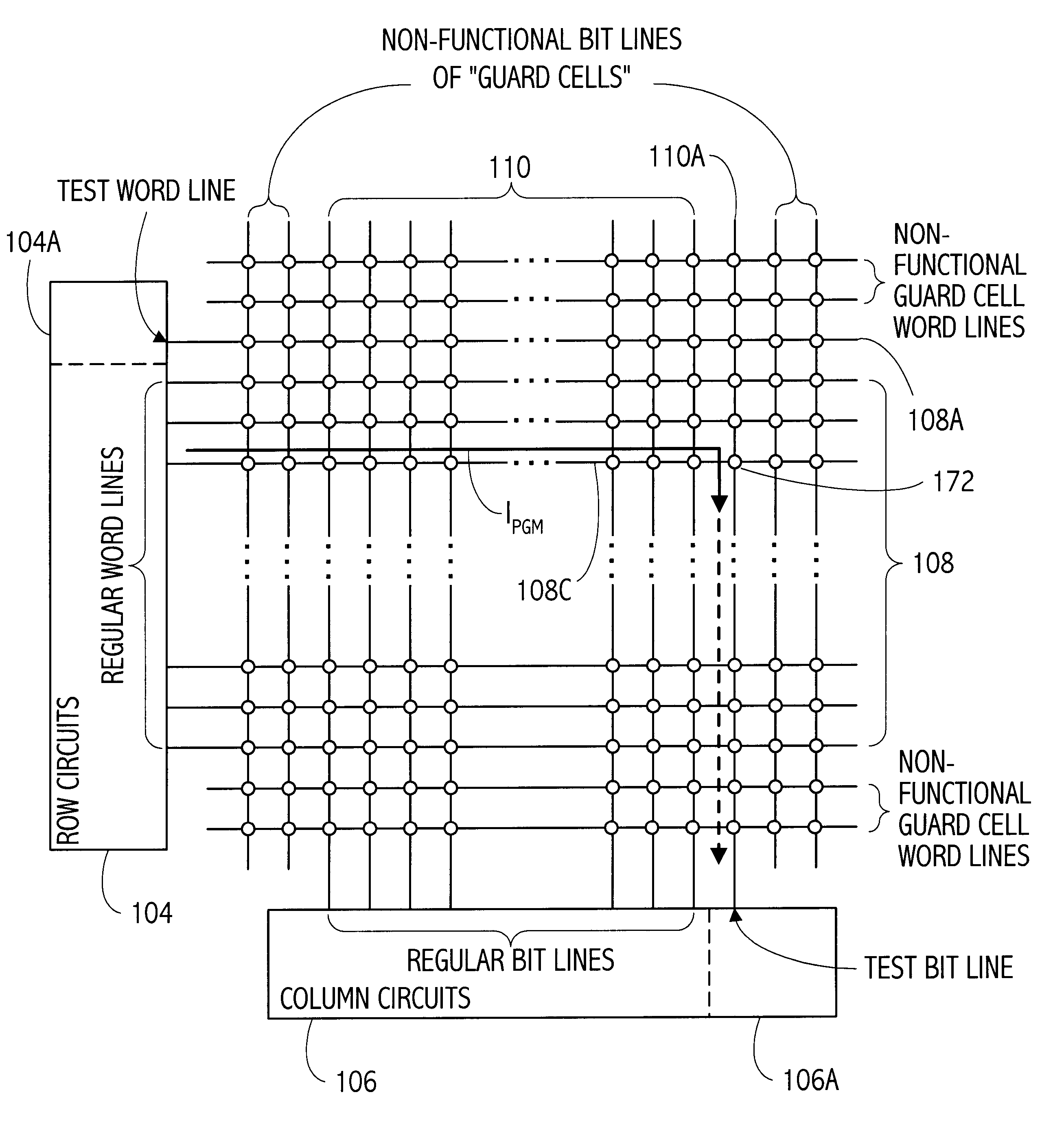
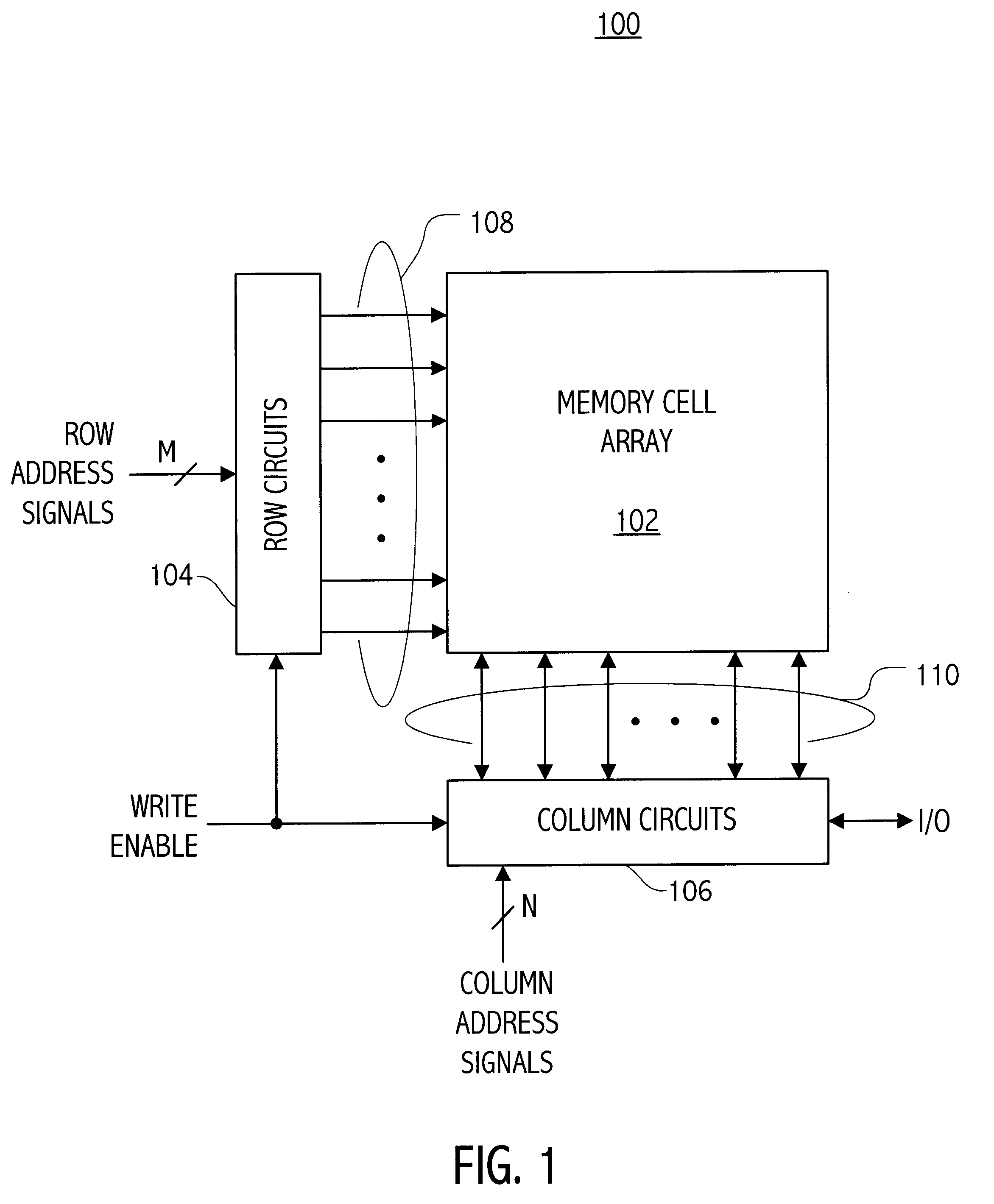
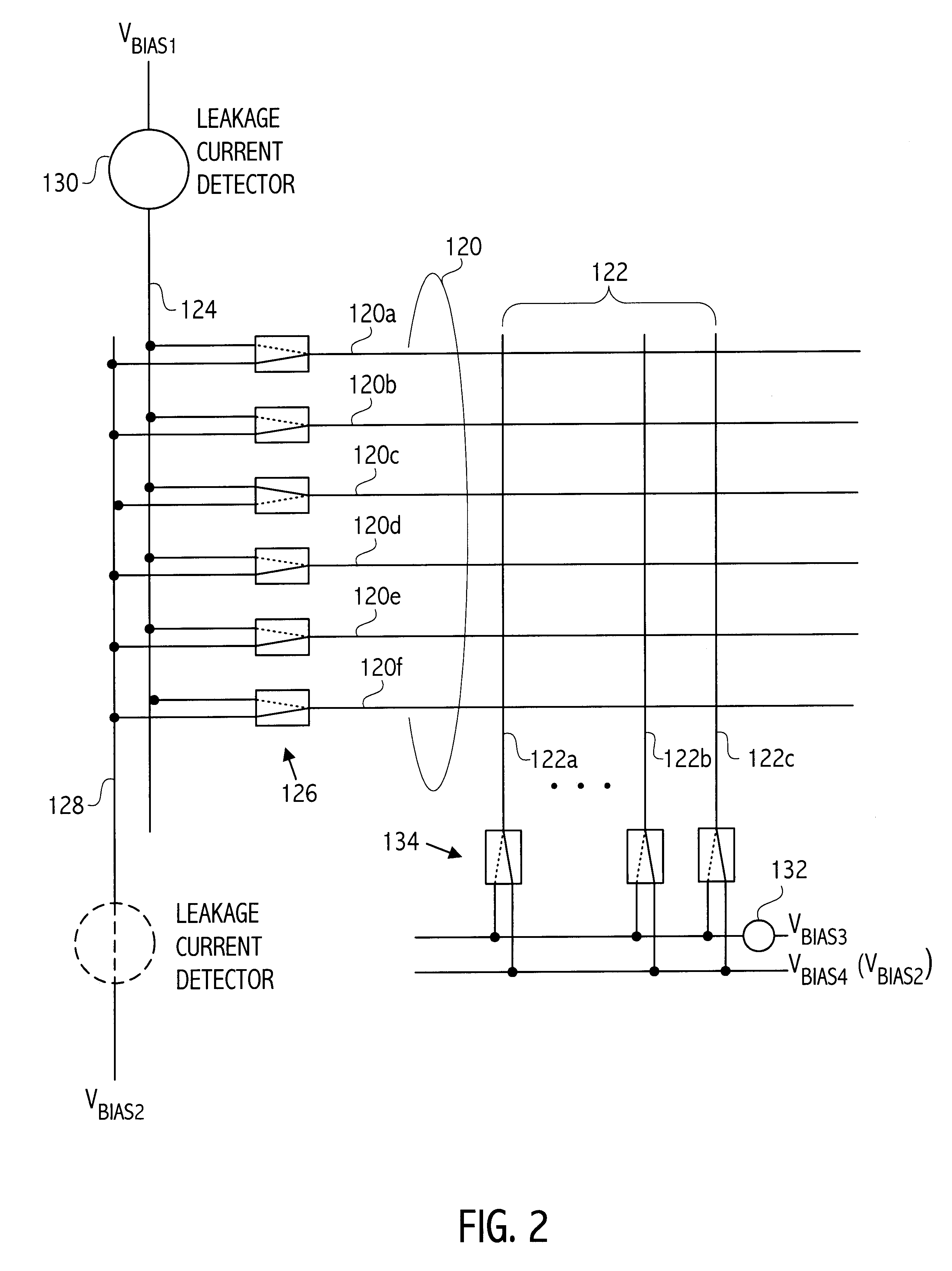
Referring now to FIG. 1, a block diagram is shown of an integrated circuit 100 including a memory array 102, which diagram may be useful to depict several preferred embodiments of the present invention. In one such embodiment, the memory array 102 is preferably a three-dimensional, field-programmable, non-volatile memory array having more than one level of memory cells, and which utilizes a read voltage different in magnitude from a write voltage. Preferred three-dimensional memory arrays are disclosed in commonly-assigned U.S. Pat. No. 6,034,882, entitled "Vertically Stacked Field Programmable Nonvolatile Memory and Method of Fabrication," which patent is incorporated herein by reference in its entirety. Another preferred three-dimensional, field-programmable, non-volatile memory array technology is disclosed in co-pending, commonly-assigned U.S. patent application Ser. No. 09 / 560,626, entitled "Three-Dimensional Memory Array and Method of Fabrication," filed Apr. 28, 2000 and nam...
PUM
 Abstract
Description
Claims
Application Information
 - R&D
- Intellectual Property
- Life Sciences
- Materials
- Tech Scout
- Unparalleled Data Quality
- Higher Quality Content
- 60% Fewer Hallucinations
Browse by: Latest US Patents, China's latest patents, Technical Efficacy Thesaurus, Application Domain, Technology Topic, Popular Technical Reports.
© 2025 PatSnap. All rights reserved.Legal|Privacy policy|Modern Slavery Act Transparency Statement|Sitemap|About US| Contact US: help@patsnap.com


