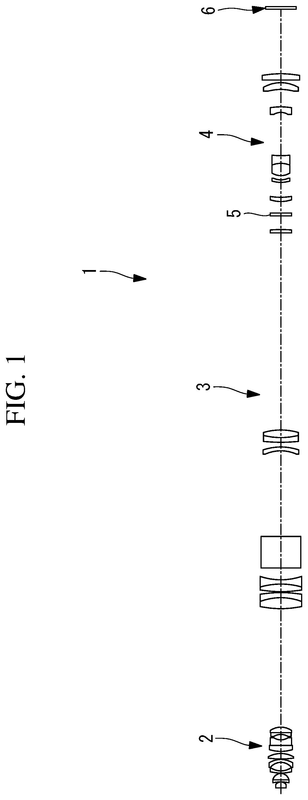
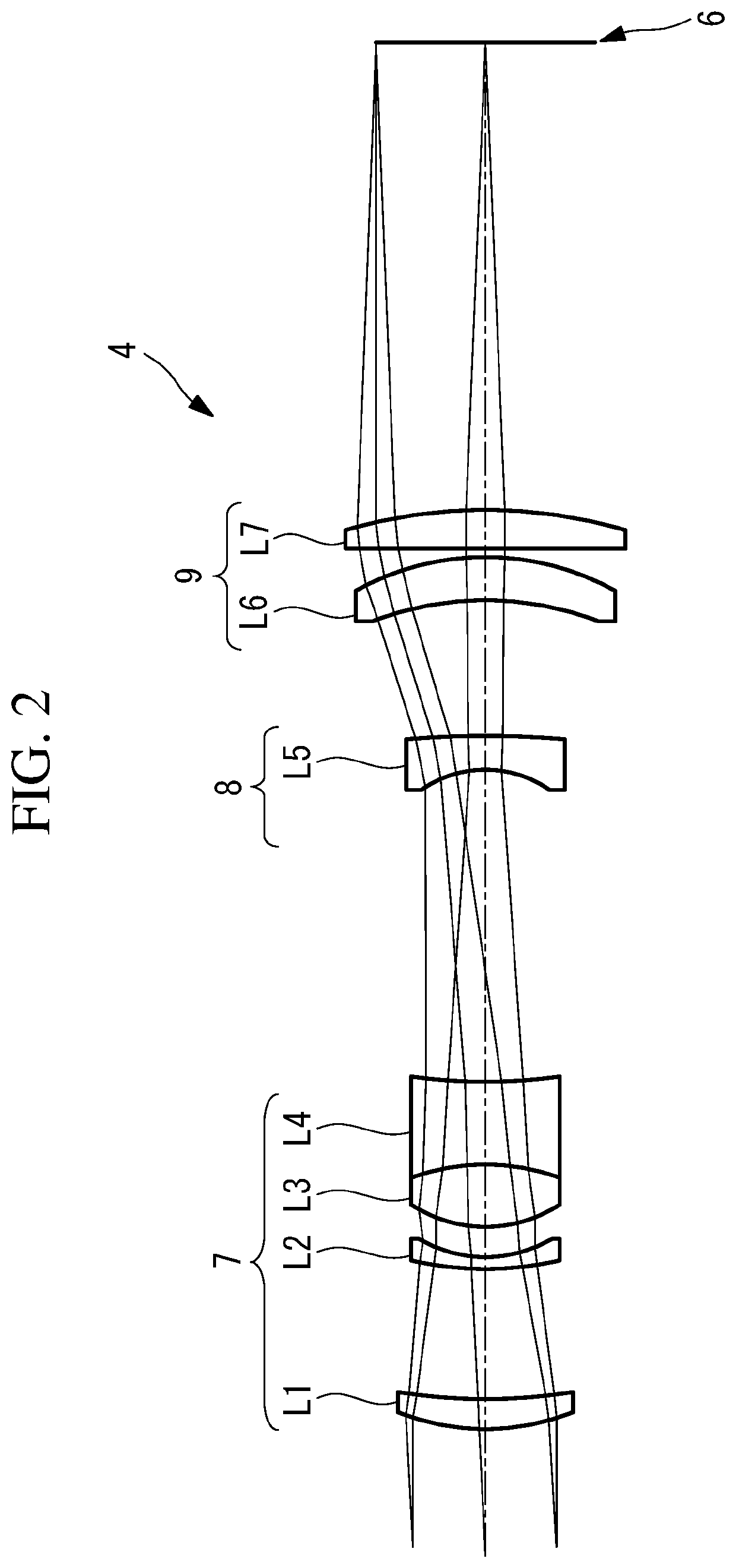
Microscope imaging optical system and light-field microscope including the microscope imaging optical system
a technology of optical system and microscope, which is applied in the field of microscope imaging optical system and light-field microscope apparatus, can solve the problem of taking a long time until the final three-dimensional information is obtained
- Summary
- Abstract
- Description
- Claims
- Application Information
AI Technical Summary
Benefits of technology
Problems solved by technology
Method used
Image
Examples
example 1
[0087]Example 1 of the microscope imaging optical system 4 according to this embodiment will be described below with reference to the drawings.
[0088]FIG. 3 is a diagram depicting the arrangement of the pupil relay optical system 3, pupil modulation optical element 5, microscope imaging optical system 4, and microlens array 6 according to this example.
[0089]Lens data of the optical system in FIG. 3 is shown below.
[0090]In addition, FIGS. 4A, 4B, and 4C show aberrations of the microscope imaging optical system 4 including the pupil relay optical system 3.
[0091]Here, the dominant wavelength is 546.07 nm, and the entrance pupil diameter is 13.5 mm.
[0092]
SurfaceRadius ofSpacing No.curvature rdndνd1∞107.0000270.27978.25001.4874970.243−46.33983.01291.8010034.974−133.00731.0398562.49456.00001.8010034.976−62.67031.50001.6541239.68738.15889.37288∞23.0001.5163364.149∞79.130010−29.12653.00001.5163364.1411−37.71861.000012162.52273.00001.6398034.471348.62676.50001.5163364.1414−50.9241170.12191551...
example 2
[0115]Example 2 of a microscope imaging optical system 12 according to this embodiment will be described below with reference to the drawings.
[0116]FIG. 7 is a diagram depicting the lens arrangement of the microscope imaging optical system 12 in this example. FIG. 8 shows the arrangement of the pupil relay optical system 3, the pupil modulation optical element 5, the microscope imaging optical system 12, and the microlens array 6.
[0117]Lens data of the optical system in FIG. 8 is shown below.
[0118]In addition, FIGS. 9A, 9B, and 9C show aberrations of the microscope imaging optical system 12 including the pupil relay optical system 3.
[0119]Here, the dominant wavelength is 546.07 nm, and the entrance pupil diameter is 13.5 mm.
[0120]
SurfaceRadius ofSpacing No.curvature rdndνd1∞125.7700261.77178.00001.4874970.243−46.77381.20001.8010034.974−139.30523.6367566.22214.46301.8010034.976−66.22211.20001.6445040.82738.01088.70008∞23.00001.5163364.149∞40.00001041.04783.00001.6889331.081123.96374....
example 3
[0149]Example 3 of a microscope pupil imaging optical system 17 according to this embodiment will be describes below with reference to the drawings.
[0150]FIG. 12 is the lens arrangement in the microscope imaging optical system 17 according to this example. FIG. 13 shows the arrangement of the pupil relay optical system 3, the pupil modulation optical element 5, the microscope imaging optical system 17, and the microlens array 6.
[0151]In this example, a light beam that comes from the object and that is collected by the finite-system microscope objective lens enters the pupil relay optical system 3 before an object image is formed.
[0152]Lens data of the optical system in FIG. 13 is shown below.
[0153]In addition, FIGS. 14A, 14B, and 14C show aberrations of the microscope imaging optical system 17 including the pupil relay optical system 3.
[0154]Here, the dominant wavelength is 546.07 nm, and the entrance pupil diameter is 20 mm.
[0155]
SurfaceRadius ofSpacing No.curvature rdndνd1∞180.000...
PUM
 Abstract
Description
Claims
Application Information
 - R&D
- Intellectual Property
- Life Sciences
- Materials
- Tech Scout
- Unparalleled Data Quality
- Higher Quality Content
- 60% Fewer Hallucinations
Browse by: Latest US Patents, China's latest patents, Technical Efficacy Thesaurus, Application Domain, Technology Topic, Popular Technical Reports.
© 2025 PatSnap. All rights reserved.Legal|Privacy policy|Modern Slavery Act Transparency Statement|Sitemap|About US| Contact US: help@patsnap.com


