Integrated control loop for linearization and temperature compensation of an electro-absorption modulator

a technology of linearization and temperature compensation, applied in the field of electro-absorption modulators, can solve the problems of significant power loss, loss of half of the drive voltage, and packaging approaches that do not meet this requiremen

Active Publication Date: 2020-01-07
ELECTROPHOTONIC IC INC
View PDF9 Cites 1 Cited by
  • Summary
  • Abstract
  • Description
  • Claims
  • Application Information

AI Technical Summary

Benefits of technology

[0007]The present invention seeks to eliminate or mitigate one or more of the above-mentioned disadvantages of known devices and systems comprising electro-absorption modulators, or at least provide an alternative.
[0013]For applications such as high speed optical data center interconnects, e.g. 25 G or 56 G and higher, it is critical that the control loop circuitry for linearization and temperature compensation provides sufficiently fast feedback and stable operation. Operation of the control loop using discrete components is not practical for high speed operation. A small die size, in which the optical components and electrical components monolithically integrated and the chip layout is optimized to place the optical and electrical components in close proximity, reduces the lengths of conductive interconnect tracks between components to microns or tens of microns, thereby reducing timing delays and phase delays.
[0015]For small form factor, low cost and relatively short reach applications, such as 400 G data center interconnects, when the control and driving electronics and the electro-absorption modulator are integrated into a sufficiently small area, it is possible to eliminate the matched impedance strip-line drive circuit and the associated power loss. Monolithic integration of the optical modulator and the associated driver and control electronics according to embodiments disclosed herein places the components in close proximity and reduces the length of conductive interconnect tracks, e.g. from millimeters to microns. This approximately 1000:1 reduction track lengths, reduces distances that electrical signals must travel, and dramatically reduces phase and time delays between blocks of components, thus enabling fast feedback control circuitry using all electronic components, or electro-optic components, to be implemented, even at very high speeds. This fast feedback approach can linearize the overall transfer function of the modulator as well as closely monitor the temperature of the modulator and apply the appropriate temperature dependent bias voltage to keep the operating range of the modulator properly centered.

Problems solved by technology

Commonly available packaging approaches do not meet this requirement and matched impedance interconnect is needed.
However, use of a matched impedance strip-lines results in significant power loss, i.e. loss of half of the drive voltage due to the matched impedances.
Another issue is that EAMs are non-linear, temperature dependent and wavelength dependent.
MZ modulators are typically larger, costlier and require a digital signal processor (DSP) or other methods to compensate for their sinusoidal modulation function.

Method used


Image

  • Integrated control loop for linearization and temperature compensation of an electro-absorption modulator
  • Integrated control loop for linearization and temperature compensation of an electro-absorption modulator

Examples


Embodiment Construction

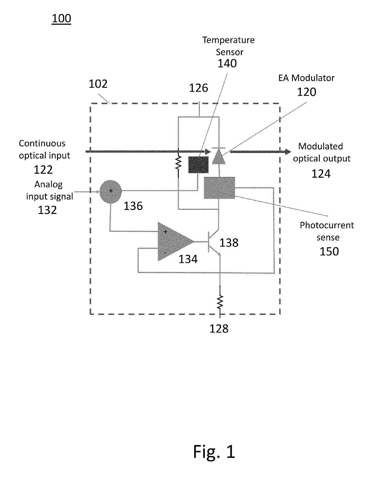
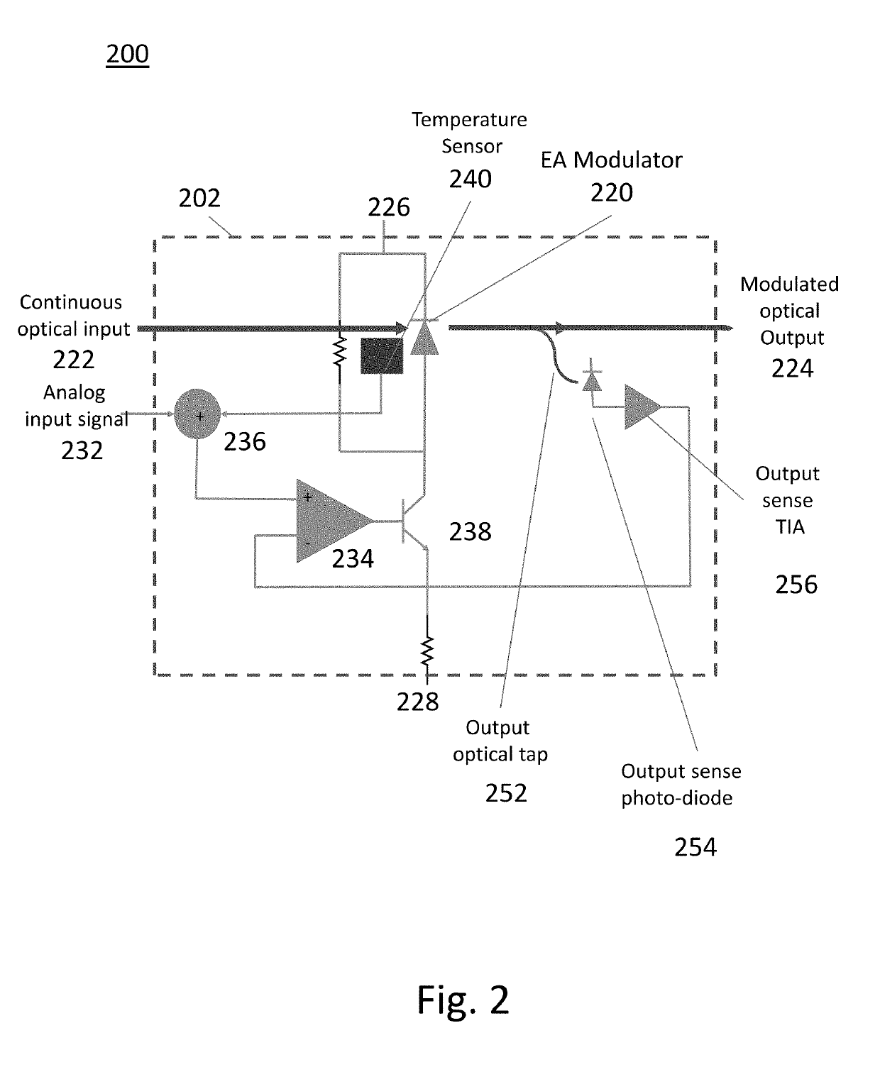
[0019]An electro-photonic integrated circuit 100 comprising an electro-absorption modulator 120 and monolithically integrated fast feedback control loop circuitry according to a first embodiment, is shown in FIG. 1. Elements of the electro-photonic integrated circuit 100 are monolithically fabricated on a device area 102 of the substrate, and comprise the electro-absorption modulator 120 and integrated driver and control circuitry elements. The electro-ab sorption modulator 120 has an optical input 122 for receiving continuous wave (CW) optical input and an optical output 124 for outputting a modulated optical output. For example, the CW optical input may be provided by a discrete or integrated laser diode (not illustrated) that is coupled to the electro-absorption modulator via an optical waveguide and / or a spot size converter (SSC). The optical output 124 may also comprise a SSC for coupling to other optical components. Electrical terminals 126 and 128 of the electro-optical modul...


PUM


Abstract

An integrated high speed electro-optical control loop for very high-speed linearization and temperature compensation of an electro-absorption modulator (EAM) for analog optical data center interconnect applications is disclosed. The control loop can function in a stable manner because the electronics and optical components are monolithically integrated on a single substrate in small form factor. Because of the small size enabled by monolithic integration, the temperatures of the optical blocks and electronics blocks are tightly coupled, and the control loop time delays and phase delays are small enough to be stable, even for very high frequency operation. This arrangement enables a low cost, low power analog transmitter implementation for data center optical interconnect applications using advanced modulation schemes, such as PAM-4 and DP-QPSK.

Description

CROSS-REFERENCE TO RELATED APPLICATIONS[0001]This application claims priority from U.S. provisional patent application No. 62 / 625,311 filed Feb. 1, 2018, entitled “Integrated Control Loop for Linearization and Temperature Compensation of an Electro-Absorption Modulator”, which is incorporated herein by reference in its entirety.TECHNICAL FIELD[0002]The present invention relates to electro-absorption modulators and particularly to linearization and temperature compensation of electro-absorption modulators for high speed optical data center applications.BACKGROUND[0003]Electro-absorption modulators (EAM) are commonly used in the fiber optics world. EAMs are used as external modulators of light output from continuous wave lasers. For example, an EAM can be used with an inexpensive slow laser for a high-performance application, i.e. transmitting at data rates limited, not by the characteristics of the laser, but by the characteristics of the EAM.[0004]In most applications of EAMs to dat...

Claims


Application Information

Patent Timeline
Patent Type & Authority Patents(United States)
IPC IPC(8): H04B10/50H04B10/588
CPCH04B10/50593H04B10/588H04B10/50575G02F1/0123G02F2203/19G02F2203/60H04B10/801
Inventor HJARTARSON, GUDMUNDUR A.HAGLEY, WILLIAM A.
Owner ELECTROPHOTONIC IC INC
Why Eureka
Try Eureka