Mounting structure and multilayer capacitor built-in substrate

a multi-layer capacitor and built-in substrate technology, applied in the direction of fixed capacitor details, stacked capacitors, printed circuit non-printed electric components association, etc., can solve the problems of vibration attributable to multi-layer ceramic capacitor distortion, mechanical distortion of multi-layer ceramic capacitor, and inapplicability, so as to reduce the noise of the circuit board, reduce the design freedom, and reduce the vibration of the entire circuit board

Active Publication Date: 2019-12-17
MURATA MFG CO LTD
View PDF18 Cites 0 Cited by
  • Summary
  • Abstract
  • Description
  • Claims
  • Application Information

AI Technical Summary

Benefits of technology

[0009]Preferred embodiments of the present invention provide mounting structures in each of which a multilayer capacitor is mounted on a circuit board and that are able to reduce vibrations of the entire circuit board so that noise from the circuit board is reduced without decreasing the design freedom, and multilayer capacitor built-in substrates that each is able to reduce vibrations of the entire multilayer capacitor built-in substrate so that noise from the circuit board is reduced without decreasing the design freedom.

Problems solved by technology

Such a high-dielectric-constant ceramic material has piezoelectric and electrostrictive properties, and thus, when voltage is applied, mechanical distortion occurs in a multilayer ceramic capacitor including a dielectric made of a high-dielectric-constant ceramic material.
Thus, when alternating-current voltage or direct-current voltage with an alternating-current component superimposed thereon is applied to the multilayer ceramic capacitor mounted on a circuit board, vibrations attributable to distortion of the multilayer ceramic capacitor are generated at the multilayer ceramic capacitor.
However, the technology disclosed in Japanese Patent Application Laid-open No. 2000-232030 is applicable only when multilayer ceramic capacitors are able to be mounted on both surfaces of the circuit board, but is not applicable when a multilayer ceramic capacitor is able to be mounted on only one surface of the circuit board.
This decreases the design freedom.

Method used


Image

  • Mounting structure and multilayer capacitor built-in substrate
  • Mounting structure and multilayer capacitor built-in substrate
  • Mounting structure and multilayer capacitor built-in substrate

Examples


first preferred embodiment

[0059]In a mounting structure according to a first preferred embodiment of the present invention, a land is provided on the surface of the second insulating layer, and the multilayer ceramic capacitor is mounted on the land on the second insulating layer. In other words, the second insulating layer having the lower Young's modulus is an insulating layer including a principal surface on which the multilayer ceramic capacitor is mounted.

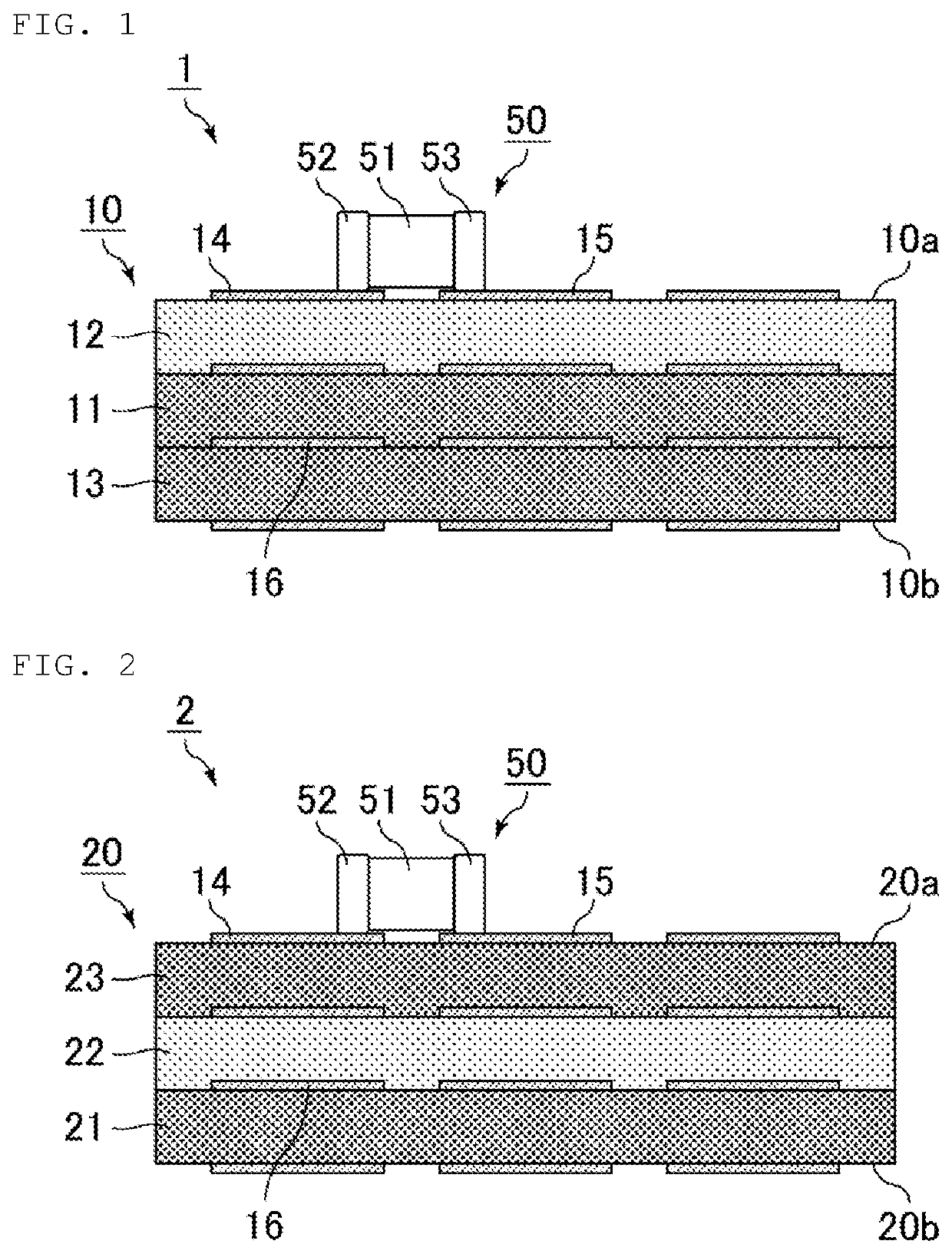
[0060]FIG. 1 is a cross-sectional view schematically illustrating the mounting structure according to the first preferred embodiment of the present invention.

[0061]The mounting structure 1 illustrated in FIG. 1 includes a circuit board 10 and a multilayer ceramic capacitor 50. The multilayer ceramic capacitor 50 is mounted on one principal surface 10a of the circuit board 10.

[0062]In FIG. 1, the multilayer ceramic capacitor 50 preferably has a rectangular or substantially rectangular parallelepiped shape as a whole and includes an element body 51 and a...

second preferred embodiment

[0093]In a mounting structure according to a second preferred embodiment of the present invention, the circuit board further includes a third insulating layer having a Young's modulus larger than that of the second insulating layer at a position closer to the principal surface on which the multilayer ceramic capacitor is mounted than the second insulating layer. In other words, the second insulating layer having the lower Young's modulus is sandwiched between the first insulating layer and the third insulating layer each having the higher Young's modulus.

[0094]The following describes a case in which a land is provided on the surface of the third insulating layer and the multilayer ceramic capacitor is mounted on the land on the third insulating layer. In this case, the third insulating layer having the higher Young's modulus is an insulating layer having a principal surface on which the multilayer ceramic capacitor is mounted.

[0095]FIG. 2 is a cross-sectional view schematically illu...

third preferred embodiment

[0115]In a multilayer capacitor built-in substrate according to a third preferred embodiment of the present invention, the resin layer on the circuit board includes a first resin layer provided on one principal surface of the circuit board, and a second resin layer provided on the first resin layer and embedding the multilayer capacitor.

[0116]In the multilayer capacitor built-in substrate according to the third preferred embodiment of the present invention, a land is provided on the surface of the second insulating layer included in the circuit board, and the multilayer ceramic capacitor is mounted on the land on the second insulating layer. In other words, the second insulating layer having the lower Young's modulus is an insulating layer having a principal surface on which the multilayer ceramic capacitor is mounted.

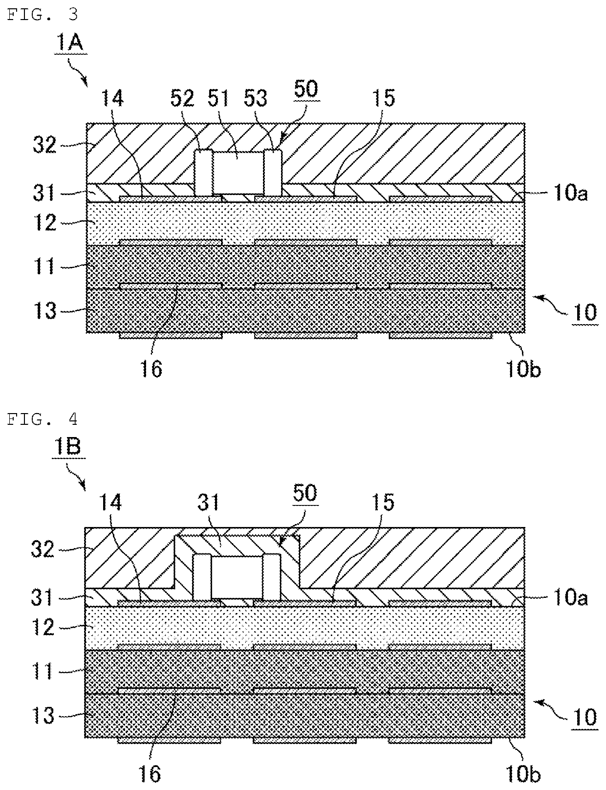
[0117]FIG. 3 is a cross-sectional view schematically illustrating an exemplary multilayer capacitor built-in substrate according to the third preferred embodiment of t...


PUM

PropertyMeasurementUnit
frequencyaaaaaaaaaa
thicknessaaaaaaaaaa
Young's modulusaaaaaaaaaa

Abstract

A mounting structure includes a circuit board including one principal surface on which a multilayer capacitor is mounted. The circuit board includes a first insulating layer, and a second insulating layer having a Young's modulus smaller than that of the first insulating layer. The second insulating layer is closer to the one principal surface than the first insulating layer. A multilayer capacitor built-in substrate includes a circuit board, a multilayer capacitor on one principal surface of the circuit board, and a resin layer on the one principal surface of the circuit board and embedding the multilayer capacitor. The circuit board includes a first insulating layer, and a second insulating layer having a Young's modulus smaller than that of the first insulating layer. The second insulating layer is closer to the one principal surface than the first insulating layer.

Description

CROSS REFERENCE TO RELATED APPLICATIONS[0001]This application claims the benefit of priority to Japanese Patent Application No. 2016-055587 filed on Mar. 18, 2016 and Japanese Patent Application No. 2016-055589 filed on Mar. 18, 2016, and is a Continuation Application of PCT Application No. PCT / JP2017 / 008325 filed on Mar. 2, 2017. The entire contents of these applications are hereby incorporated herein by reference.BACKGROUND OF THE INVENTION1. Field of the Invention[0002]The present invention relates to a mounting structure and a multilayer capacitor built-in substrate in each of which a multilayer capacitor is mounted on a circuit board.2. Description of the Related Art[0003]The capacitance of multilayer ceramic capacitors as electronic components has been increased with recent improvements in the performance of electronic devices. In a large-capacitance multilayer ceramic capacitor, a high-dielectric-constant ceramic material, such as barium titanate, is used as a dielectric mate...

Claims


Application Information

Patent Timeline
Patent Type & Authority Patents(United States)
IPC IPC(8): H01G4/30H05K1/03H01G2/06H05K1/18H01G4/005H01G4/12
CPCH01G2/06H01G4/30H05K1/181H05K1/03H01G4/12H01G4/005H05K2201/10015
Inventor YAMADA, TADATERUFUJIMOTO, ISAMUHATTORI, KAZUOTAKAHASHI, MASARU
Owner MURATA MFG CO LTD
Why Eureka
Try Eureka