White light emission

a technology of white light and light source, applied in the field of white light emission, can solve the problems of long time needed for forming p-n junction, difficulty in achieving desired color coordinates, and complex and costly preparation of oleds

Active Publication Date: 2019-06-25
MERCK PATENT GMBH
View PDF13 Cites 0 Cited by
  • Summary
  • Abstract
  • Description
  • Claims
  • Application Information

AI Technical Summary

Benefits of technology

The patent aims to provide a solution for the low performance and high complexity of white light emitting organic electroluminescent devices of the prior art. The invention provides a composition that can be easily manufactured based on standard materials and can be used as an emissive layer in thin organic electroluminescent devices. The devices show excellent performance data with respect to driving voltage, lifetime, efficiency, and color. The technical effect is the development of high-efficiency, thin, and simple organic electroluminescent devices that can be easily manufactured and suitable for mass production with high color purity.

Problems solved by technology

Single-color white OLEDs comprise one emitter with a broad emission spectrum, but achieving the desired color coordinates might be difficult with this basic approach.
The preparation of OLEDs is often quite complex and costly, as OLEDs exhibit a multi-layered structure comprising a number of different functional layers such as substrate, anode, hole injection layer (HIL), hole transport layer (HTL), emissive layer (EML), electron transport layer (ETL), electron injection layer (EIL), cathode and potentially further layers.
But the time needed for forming p-n junction is long.
In addition, lifetime of OLECs is often very short as compared to highly efficient OLEDs.
Thus, up to date OLECs aren't suitable for, e.g., display applications, but many other applications are possible such as light emitting label for, e.g. packaging.
This results in several problems such as 1) the color is very sensitive to the concentration of red emitter.
Small variations regarding the concentration can cause significant changes of the color and 2) a trace of the red emitter may also cause difficulties regarding reliability of the preparation of the polymer and 3) traces of red emitters might cause color shifts depending on the applied voltage.
White emission of such systems is either not possible or of insufficient quality.

Method used


Image

  • White light emission
  • White light emission
  • White light emission

Examples


working examples

Example 1

[0151]Materials and Preparation of Conjugated Polymers

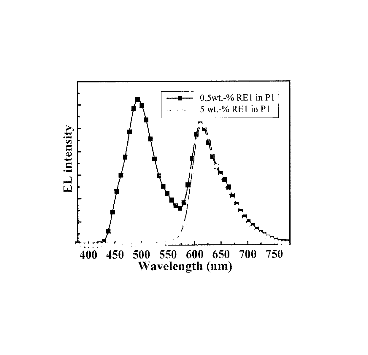
[0152]RE1 is a red light emitting phosphorescent small molecule emitter as disclosed in WO 2011 / 141120 A1

[0153]

[0154]Conjugated Polymer 1 (P1)

[0155]

[0156]P1 can be prepared according to WO 97 / 39045, WO 2003 / 020790, WO 2005 / 014688 using Suzuki coupling (WO 2003 / 048225).

[0157]Conjugated Polymer 2 (P2)

[0158]

wherein, m=0.5, n=0.35 and o=0.15. P2 can be prepared according to WO 98 / 27136, WO 99 / 24526, WO 98 / 25874.

[0159]Conjugated Polymer 3 (P3)

[0160]

[0161]P3 can be prepared according to WO 97 / 39045, WO 2003 / 020790, WO 2005 / 014688 using Suzuki coupling (WO 2003 / 048225).

[0162]The ion-transport material hydroxyl-endcapped trimethylolpropane ethoxylate (TMPE) and the salt LiCF3SO3 can be purchased from Aldrich (Steinheim, FRG). The salt is dried in a vacuum oven at T=473 K before use.

[0163]All materials are dissolved separately in anhydrous tetrahydrofuran at a concentration of 10 mg / ml. The active material solutions are prepared ...

example 2

[0164]Preparation of White Light Emitting OLEDs

[0165]For the OLED fabrication, poly(3,4-ethylenedioxythiophene)-poly(styrene sulfonate) (PEDOT:PSS, Clevios P VP AI 4083, Heraeus, FRG) is spin coated on top of carefully cleaned indium-tin-oxide (ITO) coated glass substrates (1.5×1.5 cm2, 20 ohms / square, Thin Film Devices, USA) at 4000 rpm for 60 s. The resulting 40 nm thick PEDOT:PSS film is dried at T=120° C. for 6 h. The active material is spin-coated from an active material solution at 2000 rpm for 60 s on top of the PEDOT:PSS layer. The resulting 120 nm thick active material is dried at T=50° C. for >5 h. The Ca cathodes (thickness: 20 nm), with an Al capping layer (thickness: 100 nm), are deposited on top of the active layer by thermal evaporation to complete the OLED structure.

[0166]Preparation of OLED1

[0167]According to the aforementioned method OLED1 having the following structure is prepared: ITO / PEDOT:PSS / P1:P2 (1.5 wt.-%):RE1 (0.8 wt.-%) / Ca / Al

[0168]Preparation of OLED2

[016...

example 3

[0170]Preparation of White Light Emitting OLECs

[0171]For the OLEC fabrication, poly(3,4-ethylenedioxythiophene)-poly(styrene sulfonate) (PEDOT:PSS, Clevios P VP AI 4083, Heraeus, FRG) is spin coated on top of carefully cleaned indium-tin-oxide (ITO) coated glass substrates (1.5×1.5 cm2, 20 ohms / square, Thin Film Devices, USA) at 4000 rpm for 60 s. The resulting 40 nm thick PEDOT:PSS film is dried at T=120° C. for 6 h. The active material is spin-coated from an active material solution at 2000 rpm for 60 s on top of the PEDOT:PSS layer. The resulting 120 nm thick active material is dried at T=50° C. for ≥5 h. Al cathodes (thickness: 100 nm) are deposited by thermal evaporation at p−4 Pa through a shadow mask to complete the OLEC structure.

[0172]Preparation of OLEC1

[0173]According to the aforementioned method OLEC1 having the following structure is prepared, wherein the mass ration of P1:P3:P2:RE1 is 100:1:1.5:1: ITO / PEDOT:PSS / P1:P3 (1.0 wt.-%):P2 (1.5 wt.-%):RE1 (1.0 wt.-%):Electroly...


PUM

PropertyMeasurementUnit
Nanoscale particle sizeaaaaaaaaaa

Abstract

The present invention relates inter alia to compositions comprising conjugated polymers and a small molecule, devices comprising the composition and the application of the devices.

Description

CROSS-REFERENCE TO RELATED APPLICATIONS[0001]This application is a national stage application (under 35 U.S.C. § 371) of PCT / EP2015 / 000561, filed Mar. 13, 2015, which claims benefit of European Application No. 14001199.0, filed Mar. 31, 2014, both of which are incorporated herein by reference in their entirety[0002]The present invention relates to compositions, formulations thereof, devices comprising the composition and the use of the devices.BACKGROUND OF THE INVENTION[0003]Commercial applications of white light emitting devices are manifold. White light emitting devices are not only used for lighting, but also in displays and as backlit. The requirements for modern white light emitting devices demand the development of new technologies. Displays in smartphones, tablet computers, TVs, and modern thin lighting devices, for instance, require thin and potentially flexible light sources with excellent performance characteristics. Thin electroluminescent organic light emitting devices,...

Claims


Application Information

Patent Timeline
IPC IPC(8): C09K11/02C09K11/06H01L51/00H01L51/50
CPCH01L51/0035C09K11/06H01L51/0037H01L51/0043H01L51/5036C09K11/025Y02B20/181C09K2211/1007C09K2211/1014C09K2211/1022C09K2211/1044C09K2211/1408C09K2211/1416C09K2211/1425C09K2211/1433C09K2211/185H01L51/0039H01L51/5016H01L51/5032H01L2251/308H01L2251/5376Y02B20/00H10K85/1135H10K85/115H10K85/151H10K50/135H10K50/125H10K2101/27H10K2102/103H10K85/111H10K50/11H10K2101/10
Inventor PAN, JUNYOUBUCHHOLZ, HERWIGEDMAN, LUDVIGTANG, SHI
Owner MERCK PATENT GMBH
Why Eureka
Try Eureka