LED with the current transfer penetration-enhanced window layer structure
A technology of light-emitting diodes and window layers, applied in circuits, electrical components, semiconductor devices, etc., can solve the problems of large current density under electrodes, large difference in refractive index, affecting device performance, etc., to reduce growth time and current consumption. , the effect of high light efficiency
- Summary
- Abstract
- Description
- Claims
- Application Information
AI Technical Summary
Problems solved by technology
Method used
Image

Examples
Embodiment 1
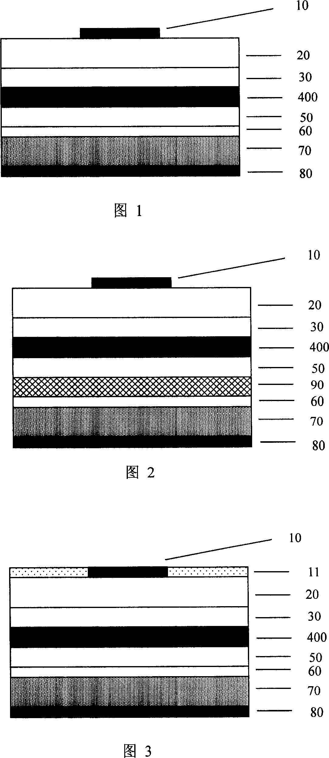
[0046] As shown in Figure 6, take AlGaInP LED as an example. The device consists of the following parts: p-type electrode 100, p-type current spreading layer 200, p-type upper confinement layer 300, active region 400, n-type lower confinement layer 500, n-type buffer layer 600, N-type substrate 700, n-type lower electrode 800, and p-type current transport anti-reflection window layer 140 composed of p-type conductive light-transmitting layer 130, current blocking layer 120 and p-type current spreading layer 200 ; Its preparation process and method are as follows:
[0047] 1. On an n-type substrate 700 formed of GaAs and other materials that can match AlGaInP, use MOVCD method to epitaxially grow n-type buffer layer 600, n-type lower confinement layer 500, active region 400, p-type An upper confinement layer 300, a p-type current spreading layer 200, thus obtaining an epitaxial wafer of an AlGaInP light-emitting diode;
[0048] 2. The specific process steps are: firstly, the ...
Embodiment 2
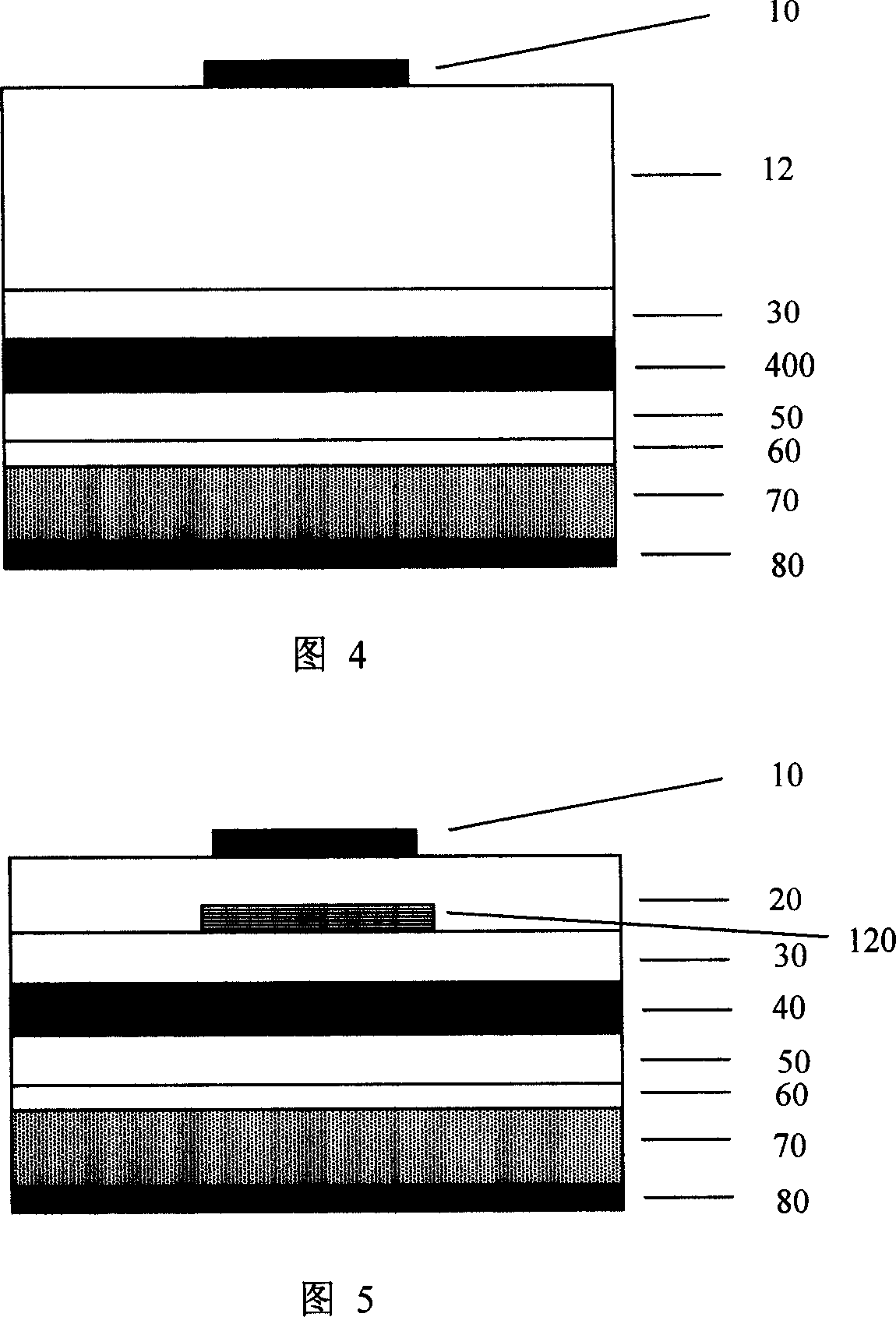
[0052] As shown in Figure 7, take AlGaInP LED as an example. The device consists of the following parts: p-type electrode 100, p-type current spreading layer 200, p-type upper confinement layer 300, active region 400, n-type lower confinement layer 500, n-type buffer layer 600, n-type substrate 700, n-type lower electrode 800, n-type DBR reflective layer 900, and p-type conductive light-transmitting layer 130, current blocking layer 120 and p-type current spreading layer 200 composed of p-type The current transport anti-reflection window layer 140; its preparation process and method are as follows:
[0053] 1. On the n-type substrate 700 formed by GaAs and other materials that can match AlGaInP, the n-type buffer layer 600, the n-type DBR light-reflecting layer 900, and the n-type lower confinement layer 500 are sequentially grown by MOVCD method, The active region 400, the p-type upper confinement layer 300, and the p-type current spreading layer 200, thus obtaining the epit...
Embodiment 3
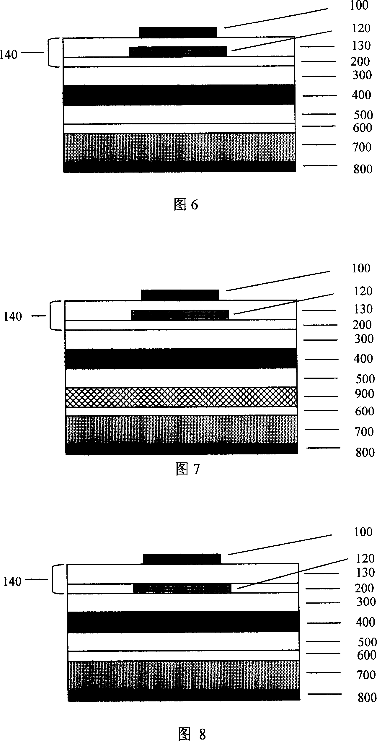
[0058] As shown in Figure 8, take AlGaInP LED as an example. The device consists of the following parts: p-type electrode 100, p-type current spreading layer 200, p-type upper confinement layer 300, active region 400, n-type lower confinement layer 500, n-type buffer layer 600, n-type substrate 700, n-type electrode 800, n-type DBR reflective layer 900, and the p-type current formed by p-type conductive light-transmitting layer 130, current blocking layer 120 and p-type current spreading layer 200 Transport window layer 140; its preparation process and method are as follows:
[0059] 1. On an n-type substrate 700 formed of GaAs and other materials that can match AlGaInP, use MOVCD method to epitaxially grow n-type buffer layer 600, n-type lower confinement layer 500, active region 400, p-type An upper confinement layer 300, a p-type current spreading layer 200, thus obtaining an epitaxial wafer of an AlGaInP light-emitting diode;
[0060] 2. The method of post-processing: fi...
PUM
 Abstract
Description
Claims
Application Information
 - R&D
- Intellectual Property
- Life Sciences
- Materials
- Tech Scout
- Unparalleled Data Quality
- Higher Quality Content
- 60% Fewer Hallucinations
Browse by: Latest US Patents, China's latest patents, Technical Efficacy Thesaurus, Application Domain, Technology Topic, Popular Technical Reports.
© 2025 PatSnap. All rights reserved.Legal|Privacy policy|Modern Slavery Act Transparency Statement|Sitemap|About US| Contact US: help@patsnap.com