Carbon nano tube film-based solar energy battery and its preparing method
A technology of carbon nanotube film and solar cell, which is applied in the direction of nanotechnology, nanotechnology, and nanotechnology for information processing, can solve the problems of low service life, complicated manufacturing process, and low conversion efficiency of solar cells, and achieve improved The effect of service life, simple preparation method and low manufacturing cost
- Summary
- Abstract
- Description
- Claims
- Application Information
AI Technical Summary
Problems solved by technology
Method used
Image
Examples
Embodiment 1
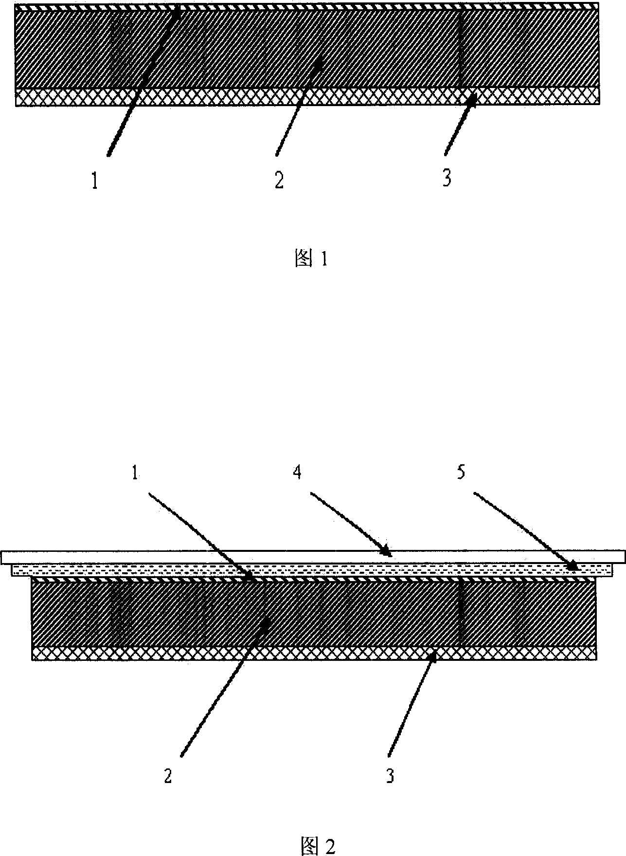
[0030] (1) Use silver glue to stick the copper mesh on the surface of one side of the silicon chip substrate 2, solidify for 24 hours, use it as the back electrode 3 of the carbon nanotube thin film solar cell, and lead it out with a wire;
[0031] (2) Place the purified double-walled carbon nanotubes in deionized water. At this time, the carbon nanotubes are agglomerated, and an ethanol solution is added dropwise thereon, and the double-walled carbon nanotubes are spread into a film with a thickness of 100 nm;
[0032] (3) transfer the double-walled carbon nanotube film after spreading to the side surface of the silicon wafer substrate 2 where the back electrode 3 is not prepared;
[0033] (4) The double-walled carbon nanotube film is dried under an infrared lamp, and the double-walled carbon nanotube film is in close contact with the silicon wafer substrate. The double-walled carbon nanotube film is used as the upper electrode of the solar cell, and is led out by wires.
[...
Embodiment 2
[0036] (1) Use silver glue to stick the copper mesh on the surface of the silicon chip substrate 2, and bake the copper mesh for 3 hours under an infrared lamp to solidify it as the back electrode 3 of the carbon nanotube thin film solar cell, and use Wire leads;
[0037] (2) Place the purified single-walled carbon nanotubes in deionized water. At this time, the carbon nanotubes are agglomerated, and an acetone solution is added dropwise thereon, and the single-walled carbon nanotubes are spread into a film with a thickness of 50 nm;
[0038] (3) transfer the single-walled carbon nanotube film 1 to the silicon wafer substrate 2 on the side surface where the back electrode is not prepared;
[0039] (4) Place the combination of the single-walled carbon nanotube film and the silicon wafer substrate obtained in step (3) in a drying oven at a temperature of 50° C. for 3 hours, so that the single-walled carbon nanotube film is in close contact with the silicon wafer substrate . Th...
Embodiment 3
[0042] (1) Put the slide glass 4 wiped clean with acetone into the intermediate frequency AC magnetron sputtering coating machine. With ZnO as the target material, the temperature of the glass slide is 250°C, and the background vacuum is 3.0×10 -3 Pa, argon pressure is 0.8Pa, target power density is 3W / cm 2 , deposition time 70s. A zinc-aluminum oxide film 5 with a thickness of about 100 nm is obtained by deposition;
[0043] (2) Use silver glue to stick the copper grid to the surface of the silicon wafer substrate 2, and bake the copper grid for 3 hours under an infrared lamp to solidify it as the back electrode 3 of the carbon nanotube thin film solar cell, and use Wire leads;
[0044] (3) Ultrasonic the prepared fixed-walled carbon nanotubes for 1 hour to fully disperse them;
[0045] (4) Transfer the fully dispersed carbon nanotubes to the surface of the silicon wafer substrate on which the back electrode is not prepared to obtain a carbon nanotube film 1 with a thickn...
PUM
| Property | Measurement | Unit |
|---|---|---|
| thickness | aaaaa | aaaaa |
| thickness | aaaaa | aaaaa |
| thickness | aaaaa | aaaaa |
Abstract
Description
Claims
Application Information
 - R&D
- Intellectual Property
- Life Sciences
- Materials
- Tech Scout
- Unparalleled Data Quality
- Higher Quality Content
- 60% Fewer Hallucinations
Browse by: Latest US Patents, China's latest patents, Technical Efficacy Thesaurus, Application Domain, Technology Topic, Popular Technical Reports.
© 2025 PatSnap. All rights reserved.Legal|Privacy policy|Modern Slavery Act Transparency Statement|Sitemap|About US| Contact US: help@patsnap.com


