Light emitting diode and its producing method

A technology of light emitting diodes and anode electrodes, which is applied to electrical components, circuits, semiconductor devices, etc., can solve the problems of low luminous efficiency and high cost of light emitting diodes, and achieve the effects of low cost, high luminous efficiency and obvious quantum effect.

Inactive Publication Date: 2012-07-04
INNOCOM TECH (SHENZHEN) CO LTD +1
View PDF0 Cites 0 Cited by
  • Summary
  • Abstract
  • Description
  • Claims
  • Application Information

AI Technical Summary

Problems solved by technology

[0010] In order to overcome the problems of low luminous efficiency and high cost of light-emitting diodes in the prior art, the present invention provides a method for making the light-emitting diode

Method used


Image

  • Light emitting diode and its producing method
  • Light emitting diode and its producing method
  • Light emitting diode and its producing method

Examples


Embodiment Construction

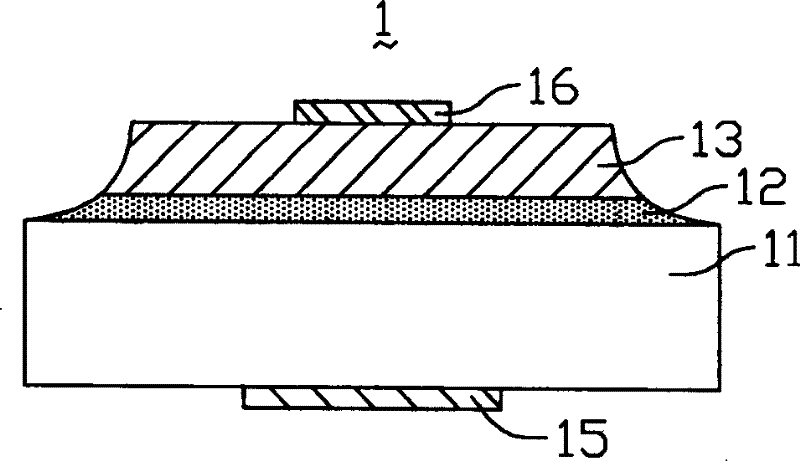
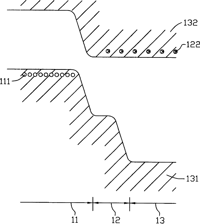
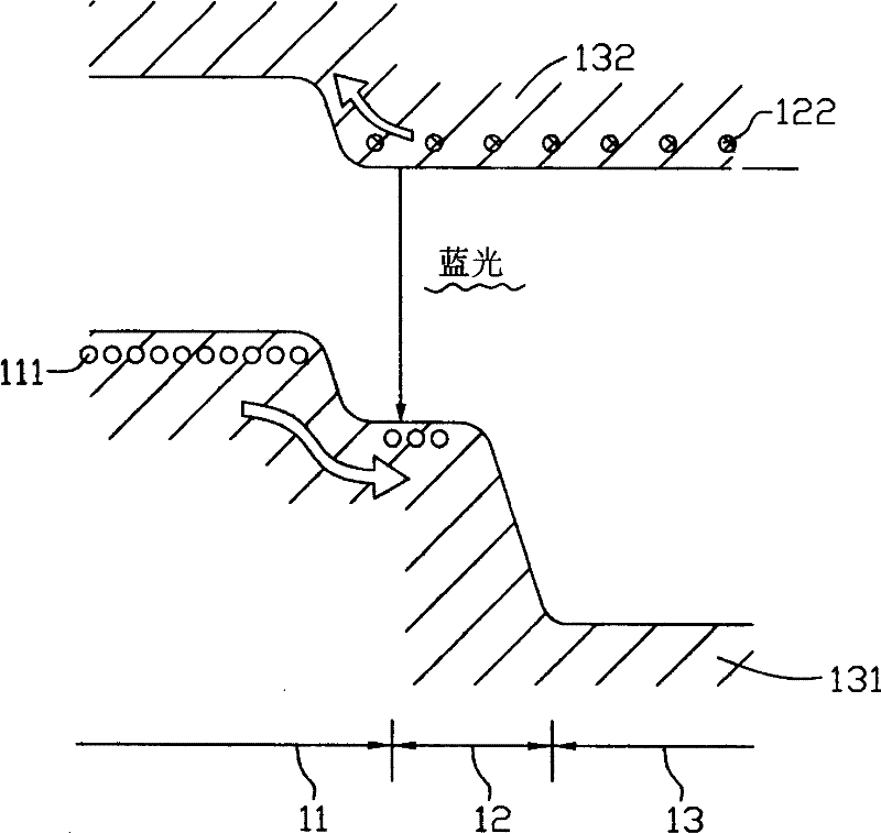
[0019] see Figure 4 , is a schematic diagram of the structure of the light-emitting diode of the present invention. The light emitting diode 2 includes a transparent substrate 21, an anode electrode 22 formed on the transparent substrate 21, an insulating layer 23 formed on the anode electrode 22, a plurality of silicon carbide alloy nanoparticles formed in the insulating layer 23 Point 24, a cathode electrode 25 formed on the insulating layer 23. Wherein, the insulating layer 23 is divided into a first insulating layer 23a and a second insulating layer 23b, and the plurality of silicon carbide alloy nano-dots 24 are located at the interface of the first insulating layer 23a and the second insulating layer 23b and form a Layered distribution. The transparent substrate 21 is made of glass or resin. The anode electrode 22 is Indium Tin Oxide (ITO) or Indium Zinc Oxide (IZO). The insulating layer 23 is silicon nitride with a thickness of 60nm to 150nm. The silicon carbide a...


PUM

PropertyMeasurementUnit
porosityaaaaaaaaaa
thicknessaaaaaaaaaa
diameteraaaaaaaaaa

Abstract

A method for producing an LED includes the following steps: a. forming an anode electrode on a transparent base board, and forming an anode electrode pattern; b. forming a first insulation layer on the anode electrode; c. forming a layer of silicon nanometer points on the first insulation layer; d. forming a layer of silicon carbide nanometer points on the silicon nanometer points; e. performing heat treatment so as to enable the silicon nanometer points and the silicon carbide nanometer points to diffuse into a layer of uniformly mixed silicon carbide alloy nanometer points; f. forming a second insulation layer on the layer of the silicon carbide alloy nanometer points; and g. forming a cathode electrode on the second insulation layer, and forming a cathode electrode pattern.

Description

【Technical field】 [0001] The invention relates to a light emitting diode and a manufacturing method thereof. 【Background technique】 [0002] In recent years, the optoelectronic industry has developed. Light Emitting Diodes (LEDs) have been widely used in display devices and optical read-write devices due to their advantages of small size, low energy consumption, high brightness, long life and stable light emission. [0003] In the production of light-emitting diodes, since the compound semiconductor is a direct bandgap semiconductor (Direct Semiconductor), it has better luminous efficiency, so the compound semiconductor is mainly used at present. However, the cost of compound semiconductors is significantly higher than that of group IV semiconductors (C, Si, Ge), so the industry is studying how to use group IV semiconductors to make light-emitting diodes. Group IV semiconductors are Indirect Semiconductors. In the theory of luminescence, because it is difficult to obey the ...

Claims


Application Information

Patent Timeline
Patent Type & Authority Patents(China)
IPC IPC(8): H01L33/00H01L33/18H01L33/34
Inventor 颜硕廷
Owner INNOCOM TECH (SHENZHEN) CO LTD
Why Eureka
Try Eureka