Packing structure with stacking platform

A packaging structure and platform technology, applied in electrical components, electrical solid devices, circuits, etc., can solve problems such as cracking of the sealant, crushing of the connected line, and reducing the production qualification rate.

Active Publication Date: 2007-04-04
ADVANCED SEMICON ENG INC
View PDF0 Cites 3 Cited by
  • Summary
  • Abstract
  • Description
  • Claims
  • Application Information

AI Technical Summary

Problems solved by technology

[0003] However, the current chip stacking technology does not provide proper protection for semi-finished chips with gold wire bonds on the substrate. Therefore, the stacked chips are easy to tilt and the connecting wires will be crushed, resulting in package failure. , reduce the production pass rate, and increase the production cost
As shown in Figure 1, since the spacer 50 only contacts the second package 30 with the surface 51, due to insufficient contact area, it is easy to make the second package 30 tilt due to loss of balance or slight vibration or impact, and press the gold wire 22 , gold wire 24 and gold wire 25, resulting in package failure
Furthermore, due to the obstruction of the spacer 50 and the gold wire 22, the gold wire 24 and the gold wire 25, it is easy to cause the sealant 40 to not completely cover each component during the mold filling process, resulting in holes, especially between the chip 23 and the spacer 50. , it is very easy to have gas holes
This hole may cause the popcorn effect (popcorn effect) during the temperature change of the subsequent process, resulting in the rupture of the sealant and reducing the product qualification rate

Method used


Image

  • Packing structure with stacking platform
  • Packing structure with stacking platform
  • Packing structure with stacking platform

Examples


Embodiment 1

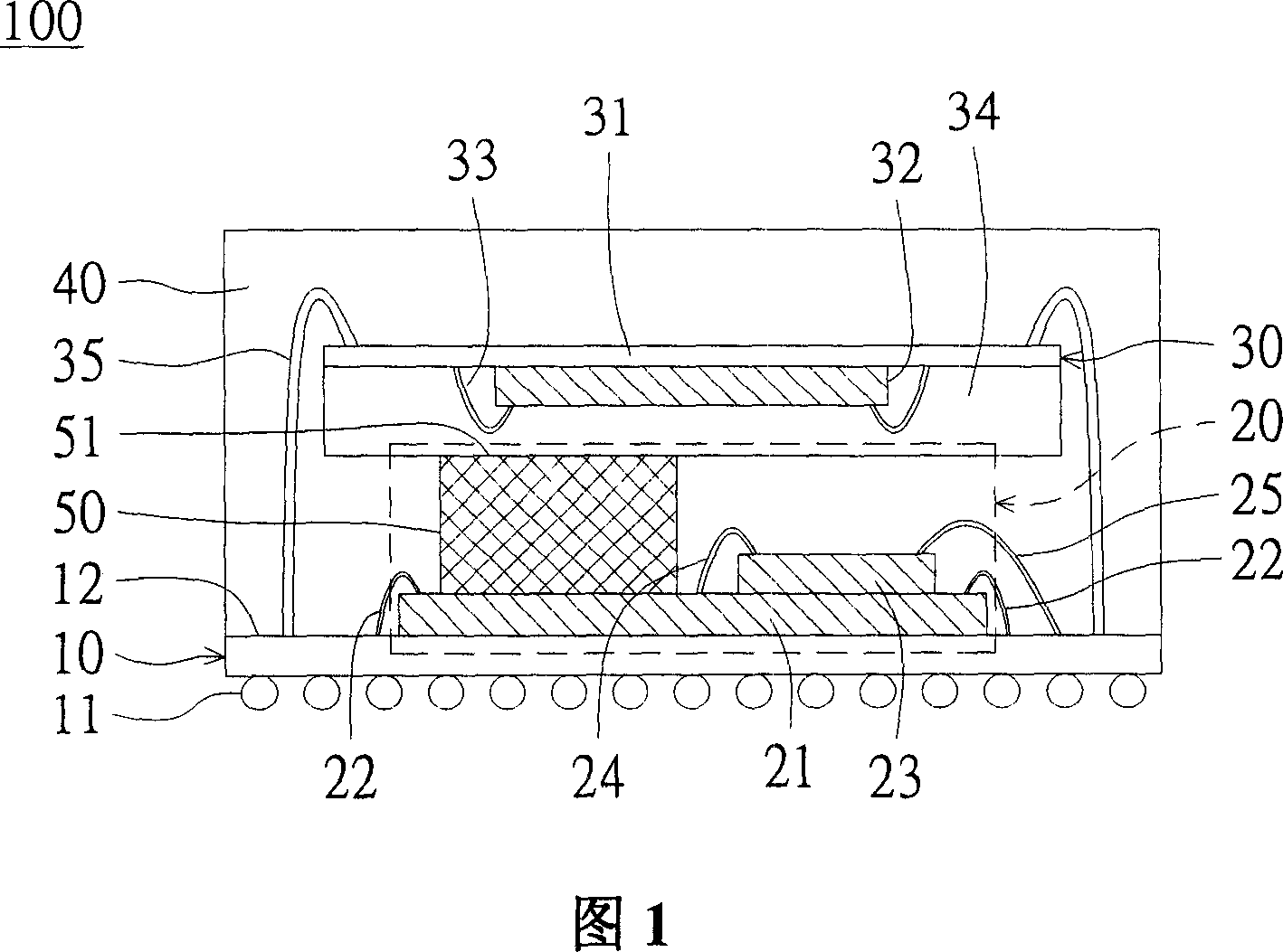
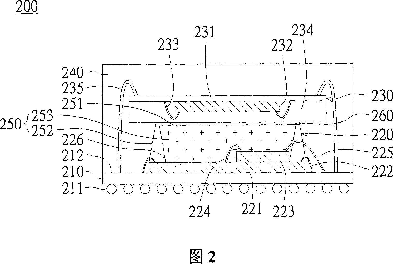
[0029] Please refer to FIG. 2 , which is a side view of a package structure according to the first embodiment of the present invention. The package structure 200 includes a substrate 210 , a first package 220 , a second package 230 and a sealant 240 . The first package 220 includes a chip 221 , a chip 223 and a liquid sealant 250 . The chip 221 is disposed on the substrate 210 and is electrically connected to the substrate 210 through gold wires 222 . The chip 223 is disposed above the chip 221 and is electrically connected to the chip 221 and the substrate 210 by gold wires 224 and gold wires 225 respectively.

[0030] The second package 230 is disposed on the platform 251 formed on the surface of the liquid encapsulant 250 . The second package 230 includes a substrate 231 and a chip 232 , the chip 232 is disposed on the substrate 231 and is electrically connected to the substrate 231 by gold wires 233 , and the second package 230 is electrically connected to the substrate 2...

Embodiment 2

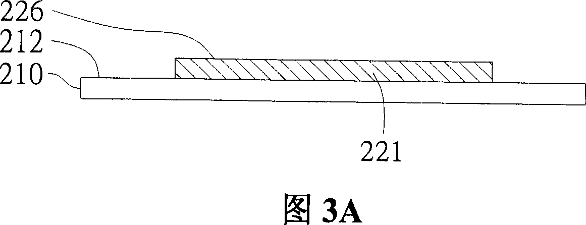
[0038]Please refer to FIG. 4 , which is a side view of the package structure of the second embodiment of the present invention. The main difference between the package structure 300 of the present embodiment and the package structure 200 of the first embodiment lies in the portion where the liquid sealant contacts the substrate. The liquid encapsulant 350 of this embodiment not only completely covers the surface 326 of the chip 321 , but also partially covers the surface 312 of the substrate 310 . The method of forming the liquid encapsulant 350 is, for example, to firstly form a dam structure 352 on the surface 312 of the substrate 310 , and the dam structure 352 is located at the periphery of a certain distance from the chip 321 . After that, the glue 353 is filled into the accommodation space surrounded by the dam 352 to form the liquid sealant 350 covering part of the surface 312 of the substrate 310 and the surface 326 of the chip 321 . The connection relationship and fo...


PUM


Abstract

The invention is concerned with the sealing structure, including: the first base panel, the first sealing piece, the second sealing piece and the sealing glue. It is: the first base panel is with the first surface; the first sealing piece includes the first CMOS chip and the liquid sealing glue; the first CMOS chip sets on the first base panel and electric connects with the first base panel by the first metal line; the liquid sealing glue covers the second surface of the first CMOS chip, and covers the first metal line partly, forms the flat at the surface of the liquid sealing glue; the second sealing piece sets on the flat, the sealing glue covers at least part of the first surface of the first base panel, the first sealing piece and the second sealing piece.

Description

technical field [0001] The present invention relates to a packaging structure, and in particular to a packaging structure with a stacking platform. Background technique [0002] With the evolution of chip packaging, the current packaging technology can complete extremely thin packaged chips. The thin chip can be packaged together with multiple thin chips using chip stacking technology to form a so-called package in package chip or multi chip module (MCM). Please refer to FIG. 1 , which is a cross-sectional view of a traditional repackaged chip structure. The package structure 100 includes a substrate 10 , a first package 20 , a second package 30 and a sealant 40 . The first package 20 includes a chip 21 , a chip 23 and a spacer 50 . The chip 21 is disposed on the substrate 10 and is electrically connected to the substrate 10 through gold wires 22 . The chip 23 is disposed above the chip 21 and is electrically connected to the chip 21 and the substrate 10 by gold wires 24 a...

Claims


Application Information

Patent Timeline
Patent Type & Authority Applications(China)
IPC IPC(8): H01L25/00H01L23/31H01L21/56
CPCH01L2924/15311H01L2224/32145H01L2924/10253H01L2224/48145H01L2224/73265H01L2224/32225H01L2924/19107H01L24/73
Inventor 林圣惟宋威岳黄文彬
Owner ADVANCED SEMICON ENG INC
Why Eureka
Try Eureka