Delay locked loop circuit

A delay-locked loop and phase-delay technology, applied in electrical components, static memory, automatic control of power, etc., can solve problems such as reduced operational reliability of semiconductor memory devices

Active Publication Date: 2007-04-04
SK HYNIX INC
View PDF0 Cites 7 Cited by
  • Summary
  • Abstract
  • Description
  • Claims
  • Application Information

AI Technical Summary

Problems solved by technology

However, if the operation margin of the DLL output clock decreases under high-frequency operation or changes in operating conditions such as pressure, temperature, or input voltage potential, when one DLL output clock with one phase is used to control multiple control circuits , the operational reliability of the semiconductor memory device decreases

Method used


Image

  • Delay locked loop circuit
  • Delay locked loop circuit
  • Delay locked loop circuit

Examples


Embodiment Construction

[0033] Hereinafter, memory devices according to specific embodiments of the present invention will be described in detail with reference to the accompanying drawings.

[0034] The semiconductor memory device according to the present invention specifically provides an enhanced delay locked loop (DLL) function.

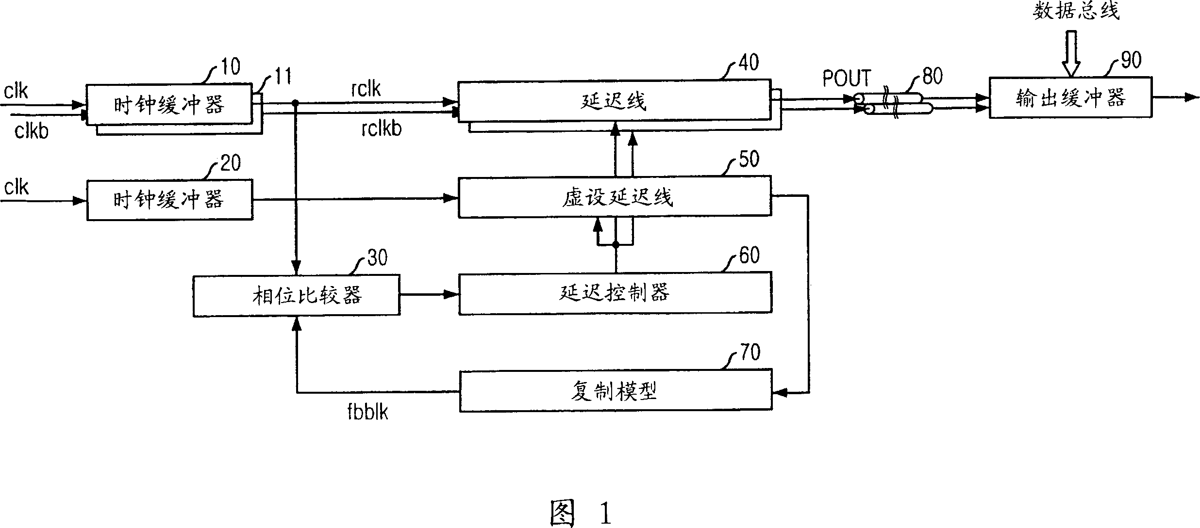
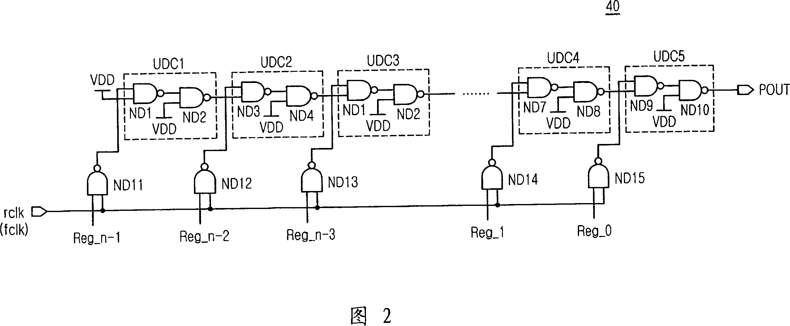
[0035] FIG. 3 is a block diagram illustrating a delay locked loop for use with a semiconductor memory device according to an embodiment of the present invention.

[0036] The delay locked loop includes: a clock delay compensation block, a phase controller 180 and a multi-phase delay controller 130 . The clock delay compensation block includes: clock buffers 100 , 101 and 110 , phase comparator 120 , delay controller 160 , multi-phase delay line 140 , dummy delay line 150 , replica model 170 and output buffer 200 .

[0037] The clock delay compensation block receives external clock signals clk and clkb to generate a first multi-clock MPCLK and a second multi-clock MPOUT...


PUM


Abstract

A delay locked loop increases an operation margin of a delay locked loop by using an output clock having more advanced phase than a DLL output clock. A clock delay compensation block receives an external clock signal to thereby generate a first multi clock and a second multi clock. A phase control block compares the first multi clock with the second multi clock to generate phase control signal controlling a shifting operation. A multi-phase delay control block performs a shifting operation based on the phase control signal to control the clock delay compensation block.

Description

technical field [0001] The present invention relates to a delay locked loop circuit; more particularly, the present invention relates to a method for controlling the output of a delay locked loop circuit in a synchronous dynamic random access memory (SDRAM) based on an operating condition such as pressure or temperature memory device. Background technique [0002] In general, a delay locked loop (DLL) is a circuit for controlling the timing of output data from a semiconductor memory device such as a dynamic random access memory (DRAM) to an external device by using an external input clock signal. In order to transfer data from a semiconductor memory device to a chipset or a CPU without any error, the output of the semiconductor memory device is synchronized with a clock signal generated from the chipset or the CPU. [0003] When a clock signal is transferred to / from an internal control block in a semiconductor memory device, the clock signal is delayed due to input clock bu...

Claims


Application Information

Patent Timeline
IPC IPC(8): G11C7/22G11C11/406G11C11/4076
CPCG11C7/1057G11C7/1066G11C7/222G11C11/4076G11C11/4093H03L7/0812H03L7/095
Inventor 金敬勋
Owner SK HYNIX INC
Why Eureka
Try Eureka