Non-volatile memory and its manufacturing method

A non-volatile, manufacturing method technology, applied in semiconductor/solid-state device manufacturing, electric solid-state devices, semiconductor devices, etc., can solve the impact, general products and methods do not have appropriate structures and methods, and affect memory operation margin components Efficiency and other issues

Active Publication Date: 2016-05-11
MACRONIX INT CO LTD
View PDF6 Cites 0 Cited by
  • Summary
  • Abstract
  • Description
  • Claims
  • Application Information

AI Technical Summary

Problems solved by technology

[0004] However, there is a second bit effect in nitride flash memory, that is, when the left bit is read, it will be affected by the right bit, or when the right bit is read, will be affected by the left bit
In addition, as the memory size gradually shrinks, the length of the channel (channel) is also shortened, causing the second bit effect to be more significant, thus affecting the operation window and device performance of the memory.
[0005] It can be seen that the above-mentioned existing non-volatile memory and its manufacturing method obviously still have inconvenience and defects in product structure, manufacturing method and use, and need to be further improved urgently.
In order to solve the above-mentioned problems, the relevant manufacturers have tried their best to find a solution, but no suitable design has been developed for a long time, and there is no suitable structure and method for general products and methods to solve the above-mentioned problems. This is obviously a problem that relevant industry players are eager to solve

Method used


Image

  • Non-volatile memory and its manufacturing method
  • Non-volatile memory and its manufacturing method
  • Non-volatile memory and its manufacturing method

Examples


Embodiment Construction

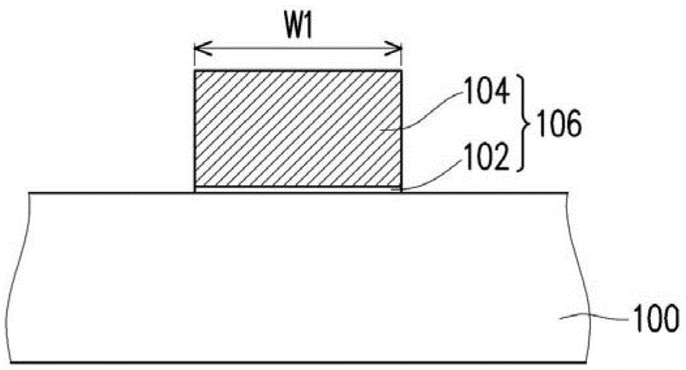
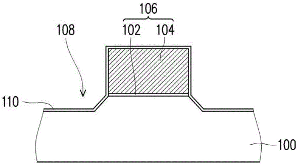
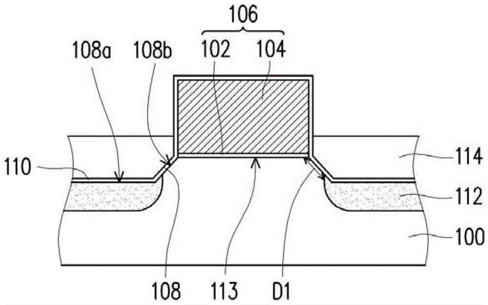
[0037] In order to further explain the technical means and effects of the present invention to achieve the intended purpose of the invention, the specific implementation and structure of the non-volatile memory and its manufacturing method according to the present invention will be described below in conjunction with the accompanying drawings and preferred embodiments. , method, step, feature and effect thereof, detailed description is as follows.

[0038] The aforementioned and other technical contents, features and effects of the present invention will be clearly presented in the following detailed description of preferred embodiments with reference to the drawings. Through the description of specific embodiments, it should be possible to obtain a deeper and more specific understanding of the technical means and effects of the present invention to achieve the intended purpose, but the attached drawings are only for reference and description, and are not used to explain the pr...


PUM


Abstract

The invention relates to a volatile memory and a fabricating method thereof. The volatile memory comprises a gate structure, a doped region, a charge storage layer and a first dielectric layer. The gate structure is arranged on the base. Recessed portions exist in the base on two sides of the gate structure. The gate structure comprises a gate dielectric layer and a gate. The gate dielectric layer is arranged on the base, and an interface exists between the gate dielectric layer and the base. The gate is arranged on the gate dielectric layer. The doped region is arranged in the based around the recessed portions. The charge storage layer is arranged in the recessed portions, and the top surface of the charge storage layer is higher than the interface. The first dielectric layer is arranged between the charge storage layer and the base and between the charge storage layer and the gate structure.

Description

technical field [0001] The invention relates to a non-volatile memory and a manufacturing method thereof, in particular to a non-volatile memory capable of avoiding second bit effects and a manufacturing method thereof. Background technique [0002] Since non-volatile memory has the advantage that the stored data will not disappear after the power is turned off, many electrical products must have this kind of memory to maintain the normal operation of the electrical product when it is turned on. In particular, flash memory (flash memory) has become a memory element widely used in personal computers and electronic devices due to its ability to perform operations such as storing, reading, and erasing data multiple times. [0003] Nitride-based flash memory (nitride-based flash memory) is a common non-volatile memory at present. In the nitride flash memory, a charge trapping structure composed of an oxide layer-nitride layer-oxide layer (that is, the well-known ONO layer) can ...

Claims


Application Information

Patent Timeline
Patent Type & Authority Patents(China)
IPC IPC(8): H01L27/115H01L21/8247
Inventor 吴冠纬
Owner MACRONIX INT CO LTD
Why Eureka
Try Eureka