Micro electromechanical system chip size airtight packaging vertical interconnecting structure and its manufacturing method

A micro-electromechanical system and hermetic packaging technology, which is applied in the direction of microstructure technology, microstructure devices, and processing microstructure devices, can solve problems such as airtightness and IC process compatibility defects, and achieve protection from damage and increase density. , Reduce the effect of on-resistance and signal interference

Inactive Publication Date: 2007-03-28
SHANGHAI INST OF MICROSYSTEM & INFORMATION TECH CHINESE ACAD OF SCI
View PDF0 Cites 26 Cited by
  • Summary
  • Abstract
  • Description
  • Claims
  • Application Information

AI Technical Summary

Problems solved by technology

There are also many methods for through-hole interconnection, such as wire bonding connection, gold bump connection, organic conductive point adhesive bonding, etc., but these methods have certain defects in terms of airtightness and IC process compatibility

Method used


Image

  • Micro electromechanical system chip size airtight packaging vertical interconnecting structure and its manufacturing method
  • Micro electromechanical system chip size airtight packaging vertical interconnecting structure and its manufacturing method
  • Micro electromechanical system chip size airtight packaging vertical interconnecting structure and its manufacturing method

Examples


Embodiment Construction

[0037] In order to fully demonstrate the advantages and positive effects of the present invention, the embodiment of n=5 and m=4 will be explained below in conjunction with the accompanying drawings, to further demonstrate the substantive features and remarkable progress of the present invention.

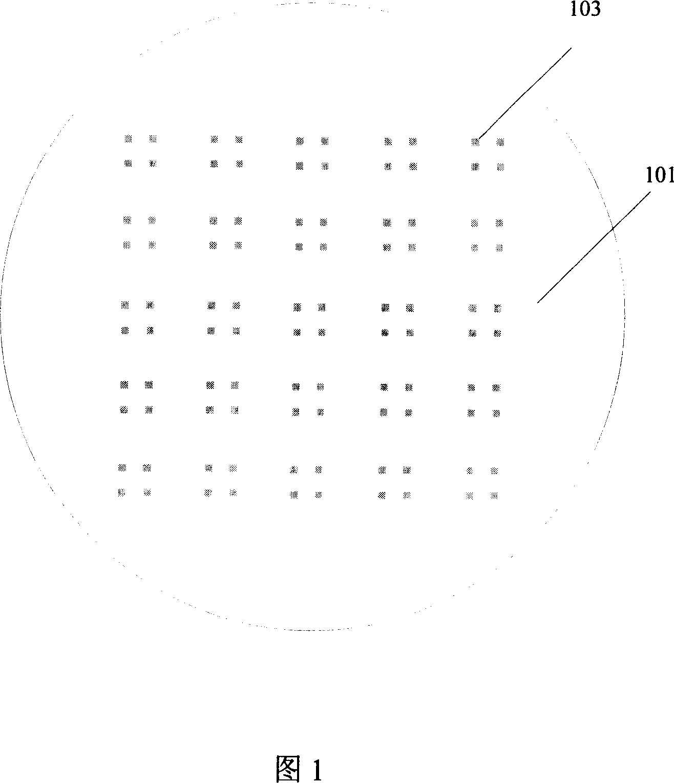
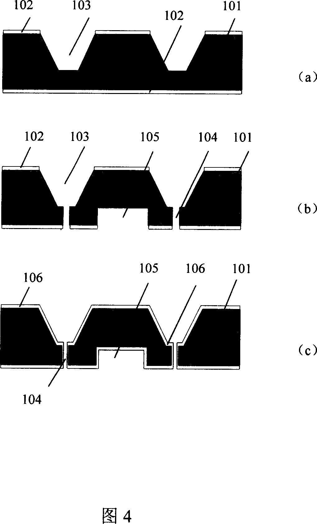
[0038] In FIG. 1 , there is a 5×5 cell array distribution on the front side of the silicon wafer 101 of the cover plate, and each cell has four inclined slots 103 , and the inclined slots 103 are formed by wet etching.

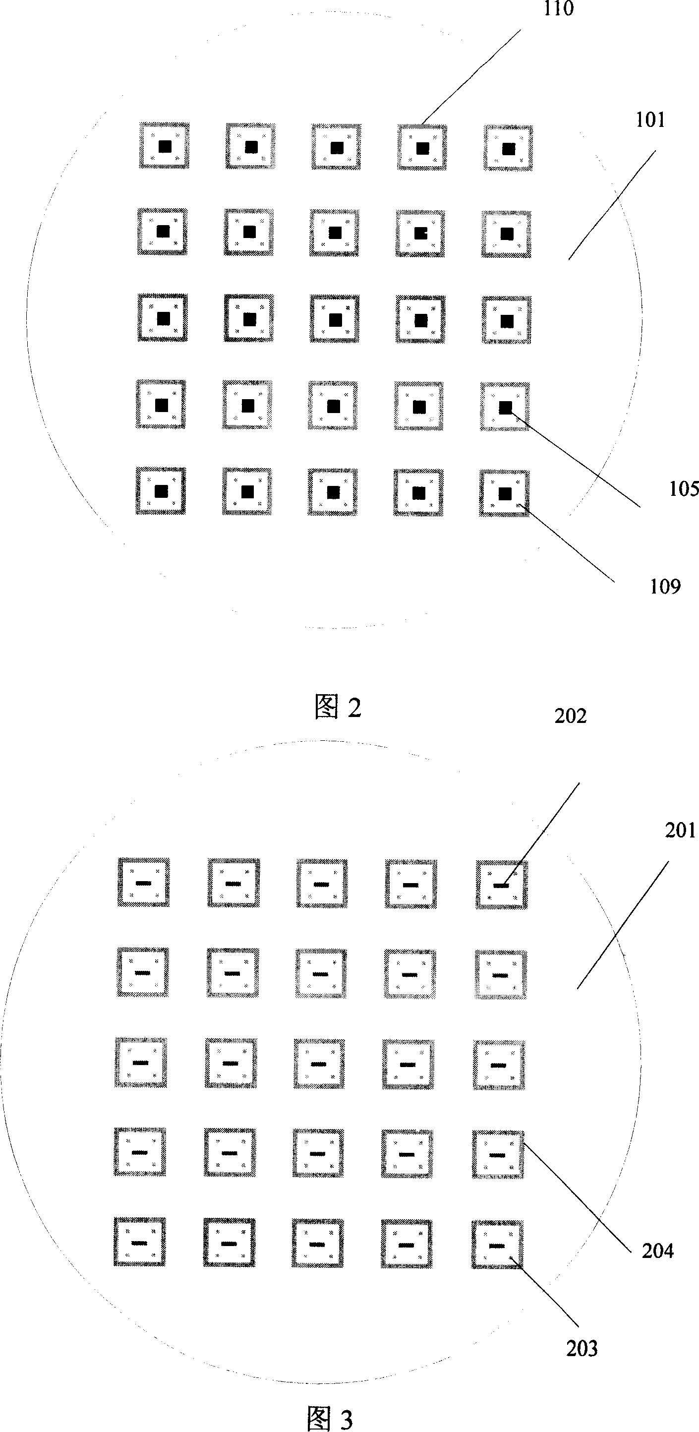
[0039] In Fig. 2, on the back of the cover silicon wafer 101 is a 5×5 cell array distribution corresponding to the front of the cover, and in the middle of each unit is a cavity 105 formed by dry etching, and around the cavity are distributed Four metal pads (pad) 109 are surrounded by a metal sealing ring 110 .

[0040] Fig. 3 is a MEMS substrate 201, inside the substrate is a 5×5 cell array distribution corresponding to the cell array distribution on the back of t...


PUM

PropertyMeasurementUnit
thicknessaaaaaaaaaa

Abstract

The invention relates to a micro electromechanical systems (MEMS) chip size airtight package vertical-interconnection structure and the making method thereof, characterized in putting forward a novel wafer-level chip size package structure, where the chip interconnection adopts through hole vertical interconnection techniques: thin silicon wafer thorugh hole etching technique of integrating KOH corrosion and DRIE, through hole metallizing technique of copper plating from the bottom up, and thorugh interconnection technique of integrating pure Sn solder airtight bonding and bump preparation. The whole process matches with IC process and is completed on the wafer-level basis, and has higher vertical thorugh hole interconnection density. And the structure reduces package cost, increases package density, and can effectively protect MEMS devices against damage, reduce impedance, parasitic effect and noise of MEMS device connection, and improve quality of output signals of MEMS devices.

Description

technical field [0001] The invention relates to a micro-electro-mechanical system chip size hermetic package vertical interconnection structure realized by vertical through-hole interconnection technology and a manufacturing method thereof, belonging to the field of MEMS device packaging. Background technique [0002] MEMS (microelectromechanical system) refers to a system made of microfabrication technology, integrating microsensors, microcomponents, microactuators, signal processing, and control circuits. MEMS devices have very broad application prospects in many fields. However, MEMS devices contain moving mechanical parts, which are fragile and easily affected by factors such as dust, air flow, moisture, machinery, etc. during the scribing and assembly process, resulting in damage to the device or the overall performance of the device The use of airtight packaging can reduce the moisture content in the package, prevent the viscous failure of MEMS devices, and improve th...

Claims


Application Information

Patent Timeline
Patent Type & Authority Applications(China)
IPC IPC(8): B81C3/00
Inventor 王玉传罗乐
Owner SHANGHAI INST OF MICROSYSTEM & INFORMATION TECH CHINESE ACAD OF SCI
Why Eureka
Try Eureka