Method for producing golden convex points with more smooth surface

A technology of surface flattening and manufacturing method, applied in the field of gold bump manufacturing, can solve the problems of high edge portion of gold bumps, affecting the reliability of semiconductor devices, rough surface of gold bumps, etc., so as to improve the packaging density and improve the pass rate and welding ability, the effect of improving integrity

Active Publication Date: 2010-04-28
SEMICON MFG INT (SHANGHAI) CORP +1
View PDF4 Cites 0 Cited by
  • Summary
  • Abstract
  • Description
  • Claims
  • Application Information

AI Technical Summary

Problems solved by technology

Roughening the gold bump surface
[0005] The surface roughness of gold bumps can negatively affect the subsequent flip-chip bonding of semiconductor chips, affecting the reliability of semiconductor devices
[0006] In the traditional gold electroplating process for manufacturing gold bumps, the current density remains unchanged throughout the electroplating process. Therefore, the thickness of the electroplated gold layer is uniform, causing the edges of the gold bumps to be higher than the central part, making the surface of the gold bumps rough
[0007] In order to overcome the shortcoming of the rough surface of the gold bump made by traditional technology, the present invention is proposed

Method used


Image

  • Method for producing golden convex points with more smooth surface
  • Method for producing golden convex points with more smooth surface
  • Method for producing golden convex points with more smooth surface

Examples


Embodiment Construction

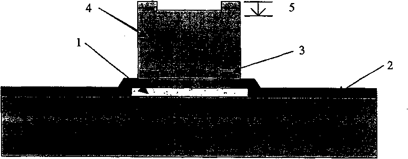
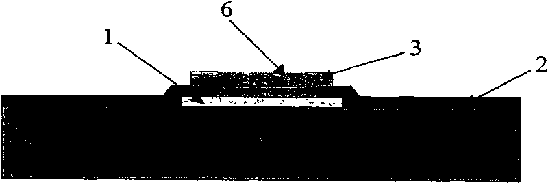
[0024] see below figure 2 and image 3 The gold bump manufacturing method according to the present invention will be described.

[0025] According to a technical solution of the present invention, the gold bump manufacturing method comprises the following steps:

[0026] Step 1, chemical vapor deposition (CVD) TiN passivation layer 2 is to be formed around the region of gold bump on the aluminum pad on the semiconductor wafer substrate, and the thickness of the TiN passivation layer 2 is 1-2 μm;

[0027] Step 2, sputtering and depositing the TiW-Au metal layer 3 under the gold bump, wherein the thickness of the TiW layer is 0.3-0.5 μm, and the thickness of the Au layer is 0.1-0.2 μm;

[0028] Step 3, electroplating on the TiW-Au metal layer 3 forms the first layer of electroplating gold (Au) layer 6, and the current density used for electroplating is 0.05-0.15 ampere / decimeter 2 ), the thickness of the formed electroplated gold layer 6 is slightly larger than the thickness...


PUM

PropertyMeasurementUnit
thicknessaaaaaaaaaa
thicknessaaaaaaaaaa
thicknessaaaaaaaaaa

Abstract

The invention is concerned with the metal bulgy point manufacture method that provides smoother surface, which uses the two galvanization craft steps with different current density to replace the traditional steps that is one galvanization craft step with one current density, it is: the first galvanization is using low current density to deposit a galvanization gold layer under the bulgy point metal layer (UBM) in order to fill the metal layer using low current density galvanization that is at the central part of the UBM layer fovea; processes the second galvanization by the high current density to form the metal protecting layer on the top of the metal bulgy point, thereby to form the smoother metal bulgy point surface structure.

Description

technical field [0001] The invention generally relates to a method for manufacturing gold bumps in electronic devices, in particular to a method for manufacturing gold bumps with smoother surfaces. Background technique [0002] In the electronics industry, gold bumps are widely used to prepare surface contacts of electronic devices, such as contacts for liquid crystal displays and semiconductor devices. The gold protective layer on the surface of gold bumps is formed by electroplating. The reason for this is that gold has high electrical conductivity, high reliability, and good resistance to chemical corrosion. [0003] However, prior to the formation of gold bump terminal electrodes, the surface of the semiconductor wafer formed by the conventional method is uneven. [0004] figure 1 is a cross-sectional view of a typical gold bump profile fabricated by conventional methods. The gold bumps include from bottom to top: aluminum pad 1, titanium nitride (TiN) passivation lay...

Claims


Application Information

Patent Timeline
Patent Type & Authority Patents(China)
IPC IPC(8): H01L21/283
Inventor 张璋炎李圣贤蒋瑞华
Owner SEMICON MFG INT (SHANGHAI) CORP
Why Eureka
Try Eureka