Semiconductor imaging device and fabrication process thereof
A technology of imaging devices and semiconductors, applied in semiconductor/solid-state device manufacturing, semiconductor devices, electric solid-state devices, etc., can solve problems such as rising and not reading signals
- Summary
- Abstract
- Description
- Claims
- Application Information
AI Technical Summary
Problems solved by technology
Method used
Image


Examples
no. 1 example
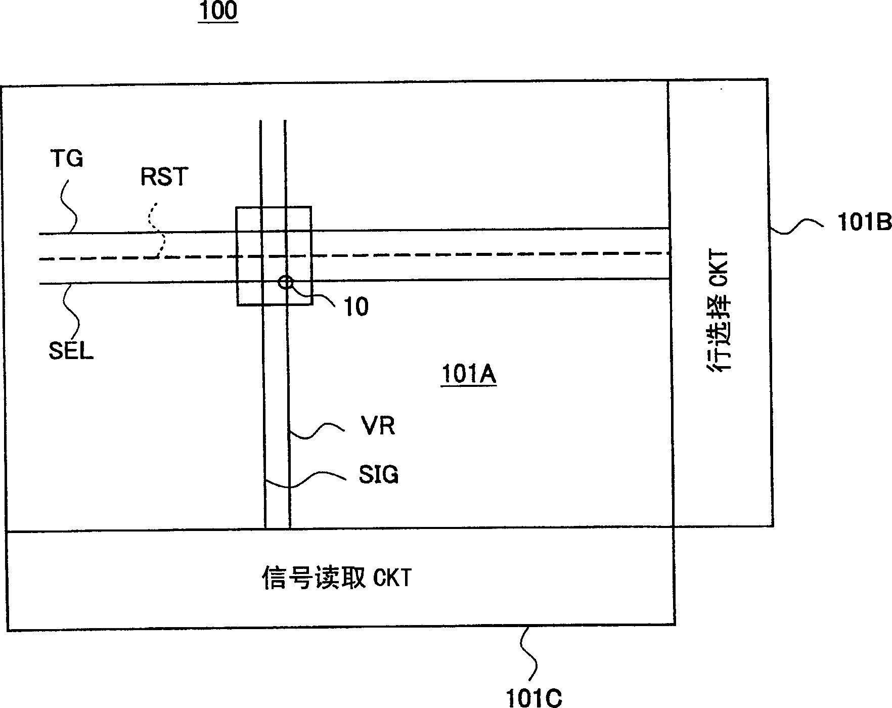
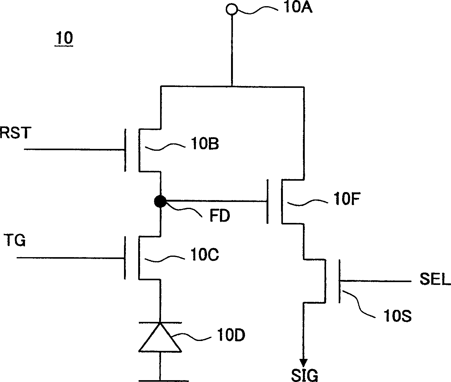
[0094] Figure 8 It is a schematic diagram showing the cross-sectional structure of the semiconductor imaging device 40 according to the first embodiment of the present invention, wherein the semiconductor imaging device 40 corresponds to figure 2 Transistor 10C and photodiode 10D of the CMOS imaging device.
[0095] refer to Figure 8 , the semiconductor imaging device 40 is formed in the p-type device region 41A defined on the silicon substrate 41 by the STI device isolation structure 41I, wherein corresponding to the channel region formed in the device region 41A, on the silicon substrate 41 via the usual A polysilicon gate electrode 43 is formed of a gate insulating film 42 which is a thermal oxide film.
[0096] In the active region 41A, an n-type diffusion region 41D is formed on the first side of the gate electrode 43 as a photodetection region of the photodiode 10D, and a p-type diffusion region 41D is formed on a surface portion of the diffusion region 41D. + Type...
no. 2 example
[0123] Figure 13A and 13B To illustrate the second embodiment according to the present invention Figure 10B A schematic diagram of a modification of the ion implantation process, while Figure 14 to show the basis Figure 13A and 13B A schematic diagram of the semiconductor imaging device 40A fabricated by the process.
[0124] refer to Figure 13A and 13B , this example will be in Figure 10B In the step of forming the p-type diffusion region 41P2, the thickness of the resist pattern R2 formed on the silicon substrate 41 is set to about 1 μm, and the surface of the n-type diffusion region 41D is at least two directions at an angle of 7 degrees. B + ion implantation.
[0125] In this case, as Figure 13B As shown, the dose of ion implantation is reduced in a shadow portion of the resist pattern R2, and a region 41pm having an intermediate impurity concentration level is formed between the p-type region 41P2 and the p-type diffusion region 41P1.
[0126] Thus, in ...
no. 3 example
[0131] Figure 15A and 15B A manufacturing process of the semiconductor imaging device 40B according to the third embodiment of the present invention is shown, wherein those parts corresponding to the foregoing parts are denoted by the same reference numerals, and their descriptions are omitted.
[0132] Figure 15A It is shown that the p-type diffusion region 41P2 is formed at a shallower level than the p-type diffusion region 41P1 Figure 10B The corresponding process of the process. For example, in Figure 15A In the step, while using the resist pattern R2 as a mask, the acceleration voltage is 8-15keV, the dose is 0.5-3.0×10 12 cm -2 And under the condition that the angle is 7 degrees, the B+ ion implantation process is performed in the relationship of overlapping with the n-type diffusion region 41D.
[0133] Due to this ion implantation process, such as Figure 15B shown in Figure 10C In the structure obtained after the step of , the p-type region 41P2 is formed...
PUM
 Abstract
Description
Claims
Application Information
 - R&D
- Intellectual Property
- Life Sciences
- Materials
- Tech Scout
- Unparalleled Data Quality
- Higher Quality Content
- 60% Fewer Hallucinations
Browse by: Latest US Patents, China's latest patents, Technical Efficacy Thesaurus, Application Domain, Technology Topic, Popular Technical Reports.
© 2025 PatSnap. All rights reserved.Legal|Privacy policy|Modern Slavery Act Transparency Statement|Sitemap|About US| Contact US: help@patsnap.com