Apparatus and method for treating semiconductor device with plasma

A technology for processing equipment and plasma, which is applied in the fields of plasma, semiconductor/solid-state device manufacturing, pharmaceutical equipment, etc., and can solve problems such as unbalanced chemical reactions, reduced etching rate, and reduced etching uniformity

Active Publication Date: 2006-10-04
SEMES CO LTD
View PDF1 Cites 4 Cited by
  • Summary
  • Abstract
  • Description
  • Claims
  • Application Information

AI Technical Summary

Problems solved by technology

If the group distribution is irregular, the chemical reaction becomes uneven, which reduces the e

Method used


Image

  • Apparatus and method for treating semiconductor device with plasma
  • Apparatus and method for treating semiconductor device with plasma
  • Apparatus and method for treating semiconductor device with plasma

Examples


Embodiment Construction

[0028] Hereinafter, preferred embodiments of the present invention will be described in more detail with reference to the accompanying drawings. However, the present invention can be implemented in different ways and is not limited to the embodiments presented here. Rather, these embodiments are provided so that this disclosure will be thorough and will fully convey the scope of the invention to those skilled in the art. Although not described in detail here, the present invention may also include various additional devices or devices. Throughout, the same reference numerals denote the same elements.

[0029] Hereinafter, exemplary embodiments of the present invention will be described with reference to the accompanying drawings.

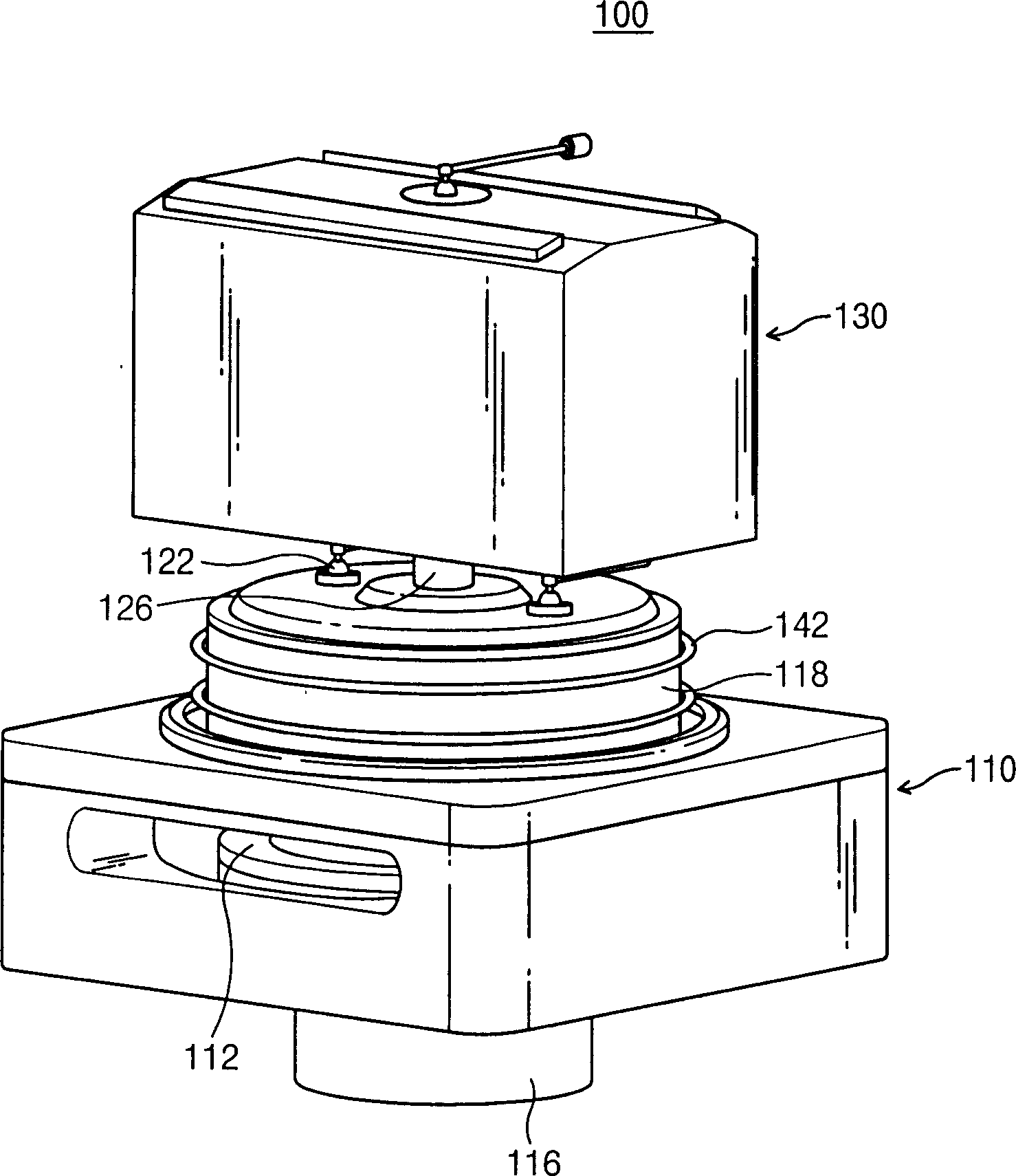
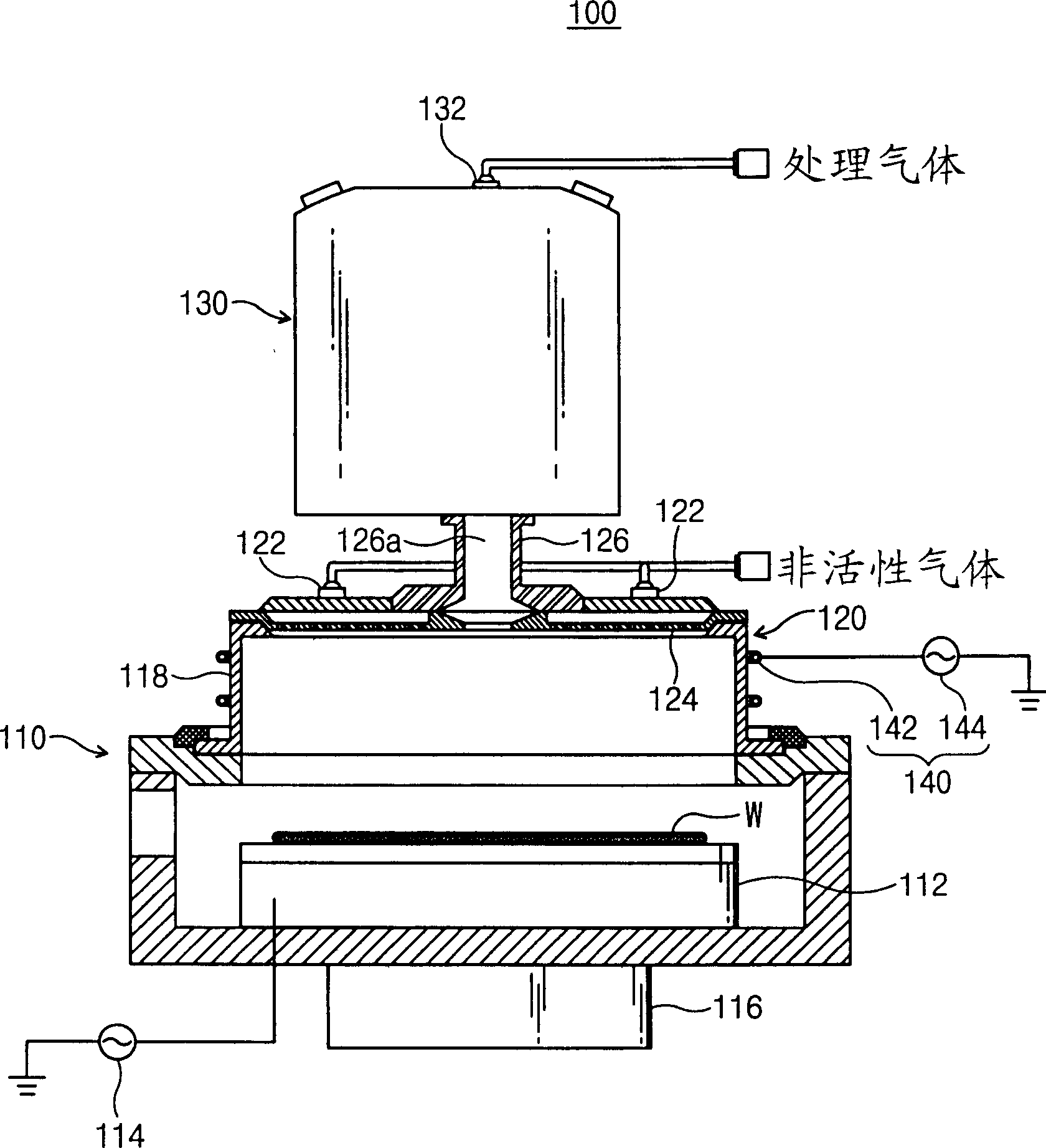
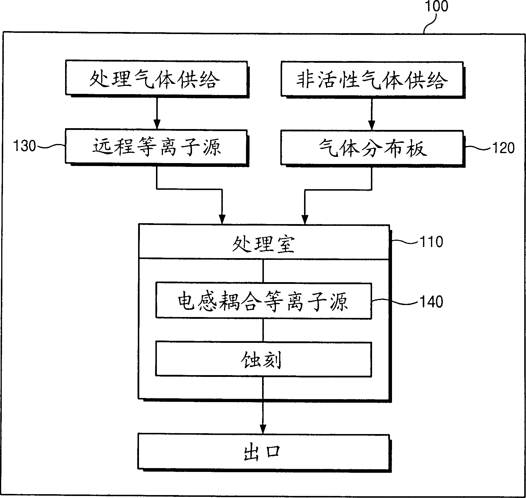
[0030] figure 1 is a perspective view showing a semiconductor plasma processing apparatus of a preferred embodiment of the present invention. figure 2 is a sectional view showing a semiconductor plasma processing apparatus of a preferred embodi...


PUM


Abstract

A semiconductor plasma-processing apparatus smoothes effects of side radical-concentration, which are frequently generated by inductive-coupling plasma sources, enhancing the etching uniformity therein. The apparatus includes a remote plasma generator providing lots of radicals and ions from activating processing gas; a reaction chamber having an inflow port through which the activated processing gas; a susceptor, on which a wafer is settled, disposed in the reaction chamber; and an inductive-coupling plasma generator disposed in the reaction chamber, providing high-frequency energy to the activated processing gas. As radicals and ions are affluently generated enough to conduct an etching process, by means of the remote and inductive-coupling plasma sources, the reaction sprightly proceeds to improve the etching efficiency.

Description

[0001] related application [0002] This application claims priority from Korean Patent Application No. 10-2005-0005790 filed on Jan. 21, 2005, the entire contents of which are incorporated herein by reference. technical field [0003] The subject matter disclosed herein relates to plasma processing equipment. Specifically, the subject matter disclosed herein relates to semiconductor plasma processing apparatus and methods that improve etch uniformity by eliminating the high concentration of side groups often produced by inductively coupled plasma sources. Background technique [0004] With the development trend of semiconductor devices toward higher integration, larger wafer size, larger LCD area, etc., the demand for high-performance equipment for processing etching processes or thin films is increasing. Furthermore, various plasma processing equipment for plasma etching, plasma enhanced CVD, and plasma ashing are also required. In other words, those devices are graduall...

Claims


Application Information

Patent Timeline
IPC IPC(8): H05H1/46H01L21/00H01L21/3065H01L21/311H01L21/3213
CPCH01J37/32357H01J37/321A61M3/0279A61M3/0262A61M3/0266A61M2205/273
Inventor 金炯俊李奇英
Owner SEMES CO LTD
Why Eureka
Try Eureka