Single-nano-thread in-situ mechanical characteristic detection and structure analysis method and apparatus
A technology for structural analysis and nanowires, which is used in measurement devices, preparation of test samples, and analysis of materials. simple effect
- Summary
- Abstract
- Description
- Claims
- Application Information
AI Technical Summary
Problems solved by technology
Method used
Image
Examples
Embodiment 1
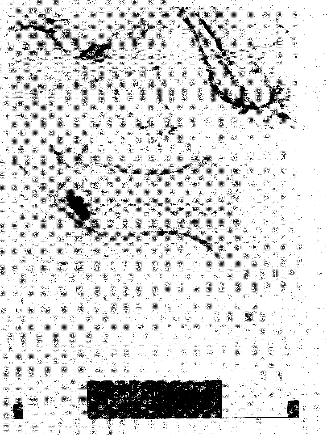
[0025] Put the Si nanowire powder in acetone and ultrasonically disperse it for 20 minutes, drop the suspension on a 100-mesh gold mesh plated with a 60nm-thick collodion support film, and fix the gold mesh on the sample rod of the transmission electron microscope. Put the sample seat into the transmission electron microscope, and adjust the electron beam current density at 2×10 at the accelerating voltage of 200KV 20 Electrons per square centimeter second, irradiating the collodion support film, the support film is curled and deformed, and the Si nanowire is bent and deformed. The diameter of the deformed nanowire is 30nm, the length is about 3μm, and the maximum strain of the nanowire is 2.5 %, the nanowires still maintain the original structure without fracture and plastic deformation, revealing that the Si nanowires have a large bending strength, figure 1 The transmission electron micrographs of the maximum bending are given, and the curled and deformed collodion support f...
Embodiment 2
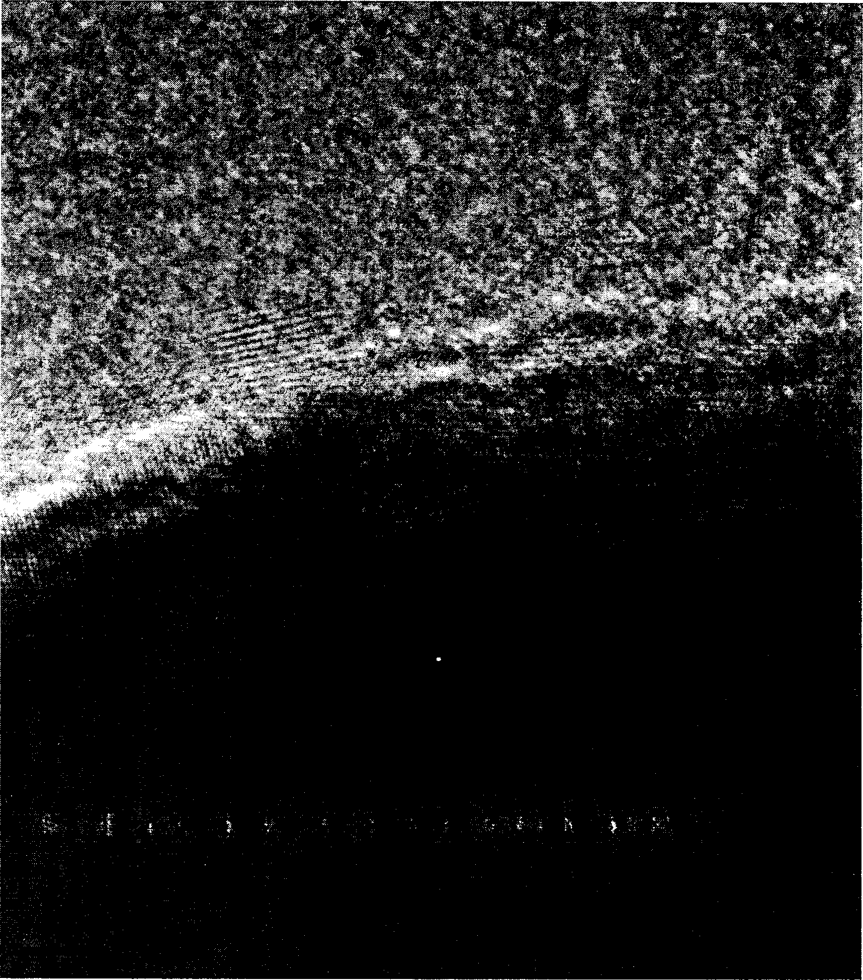
[0027] Put the SiC nanowire powder in ethanol, disperse it by ultrasonic wave for 30 minutes, drop the dispersed suspension on a 1000-mesh copper grid coated with a collodion support film, the thickness of the collodion support film is 80nm, and fix the copper grid on Put the sample holder of the transmission electron microscope sample rod into the transmission electron microscope, and adjust the electron beam current density at 1×10 at the acceleration voltage of 80KV. 20 Electrons per square centimeter second, the collodion support film is irradiated, and the support film is curled and deformed, which drives the SiC nanowires distributed on it and around it to move or bend. One of them has a diameter of 200nm and a length of 4.3μm The deformation process of the SiC nanowires was measured in situ, and one of the SiC nanowires maintained fully elastic behavior up to 2% strain, figure 2 The high-resolution atomic lattice image at the maximum bending deformation is given, showi...
Embodiment 3
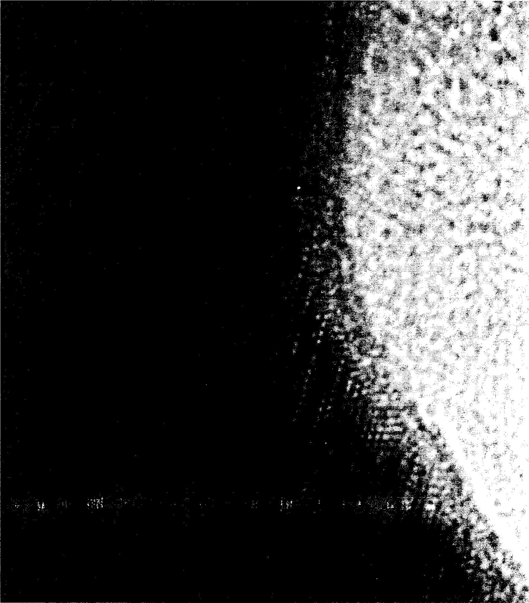
[0029] Put the SiC nanometer powder in ethanol, disperse it by ultrasonic wave for 10 minutes, drop the dispersed suspension on a 300-mesh nickel mesh coated with a collodion support film, the thickness of the collodion support film is 100nm, and fix the nickel mesh on Put the sample holder of the transmission electron microscope sample rod into the transmission electron microscope, and adjust the electron beam current density at 8×10 at the accelerating voltage of 300KV 25 Electrons / square centimeter, irradiated collodion support film, the support film was curled and deformed, a SiC nanowire with a diameter of 150nm and a length of 15μm was bent and deformed with the deformation of the support film, and the maximum bending elastic strain reached 2.0% Plastic deformation occurred later, and the process of plastic deformation of SiC nanowires was recorded in real time through high-resolution images. image 3 The high-resolution atomic lattice image shows the deformation charact...
PUM
| Property | Measurement | Unit |
|---|---|---|
| pore size | aaaaa | aaaaa |
| diameter | aaaaa | aaaaa |
| length | aaaaa | aaaaa |
Abstract
Description
Claims
Application Information
 - Generate Ideas
- Intellectual Property
- Life Sciences
- Materials
- Tech Scout
- Unparalleled Data Quality
- Higher Quality Content
- 60% Fewer Hallucinations
Browse by: Latest US Patents, China's latest patents, Technical Efficacy Thesaurus, Application Domain, Technology Topic, Popular Technical Reports.
© 2025 PatSnap. All rights reserved.Legal|Privacy policy|Modern Slavery Act Transparency Statement|Sitemap|About US| Contact US: help@patsnap.com


