Magnetically controlled sputtering process

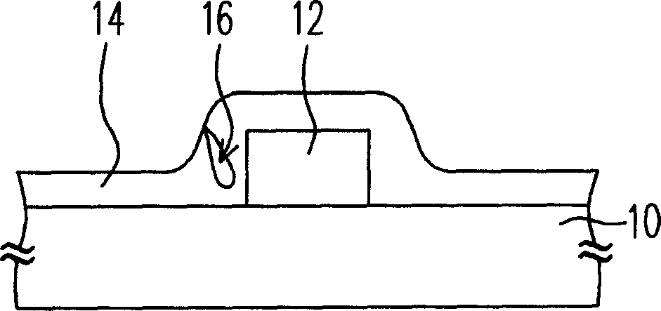
A manufacturing process and magnetron sputtering technology, applied in the field of thin film deposition manufacturing process, can solve the problems of fracture or buried hole 16, the influence of coating yield is greatly affected, and achieve the effect of improving coating yield

Inactive Publication Date: 2006-08-02
CHUNGHWA PICTURE TUBES LTD
View PDF0 Cites 9 Cited by
  • Summary
  • Abstract
  • Description
  • Claims
  • Application Information

AI Technical Summary

Problems solved by technology

Please refer to figure 2 After the film layer 12 on the substrate 10 passes through the known magnetron sputtering manufacturing process (the pressure of its reaction chamber 100 is maintained at about 1pa), its coating film 14 is easy to be formed on the side wall of the film layer 12 pattern (in the industry) Commonly known as the climbing section) breaks or buried holes 16, etc., which is commonly known in the industry as climbing disconnection phenomenon, this phenomenon will cause open circuit (open circuit), which has a great impact on the coating yield

Method used


Image

  • Magnetically controlled sputtering process
  • Magnetically controlled sputtering process
  • Magnetically controlled sputtering process

Examples


Embodiment Construction

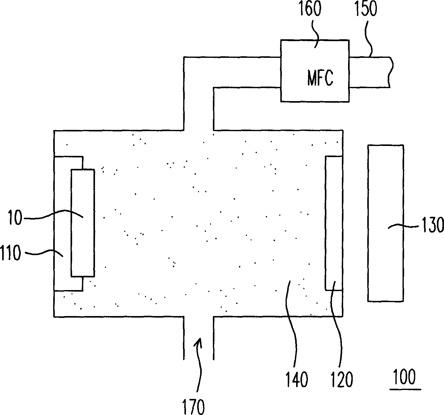
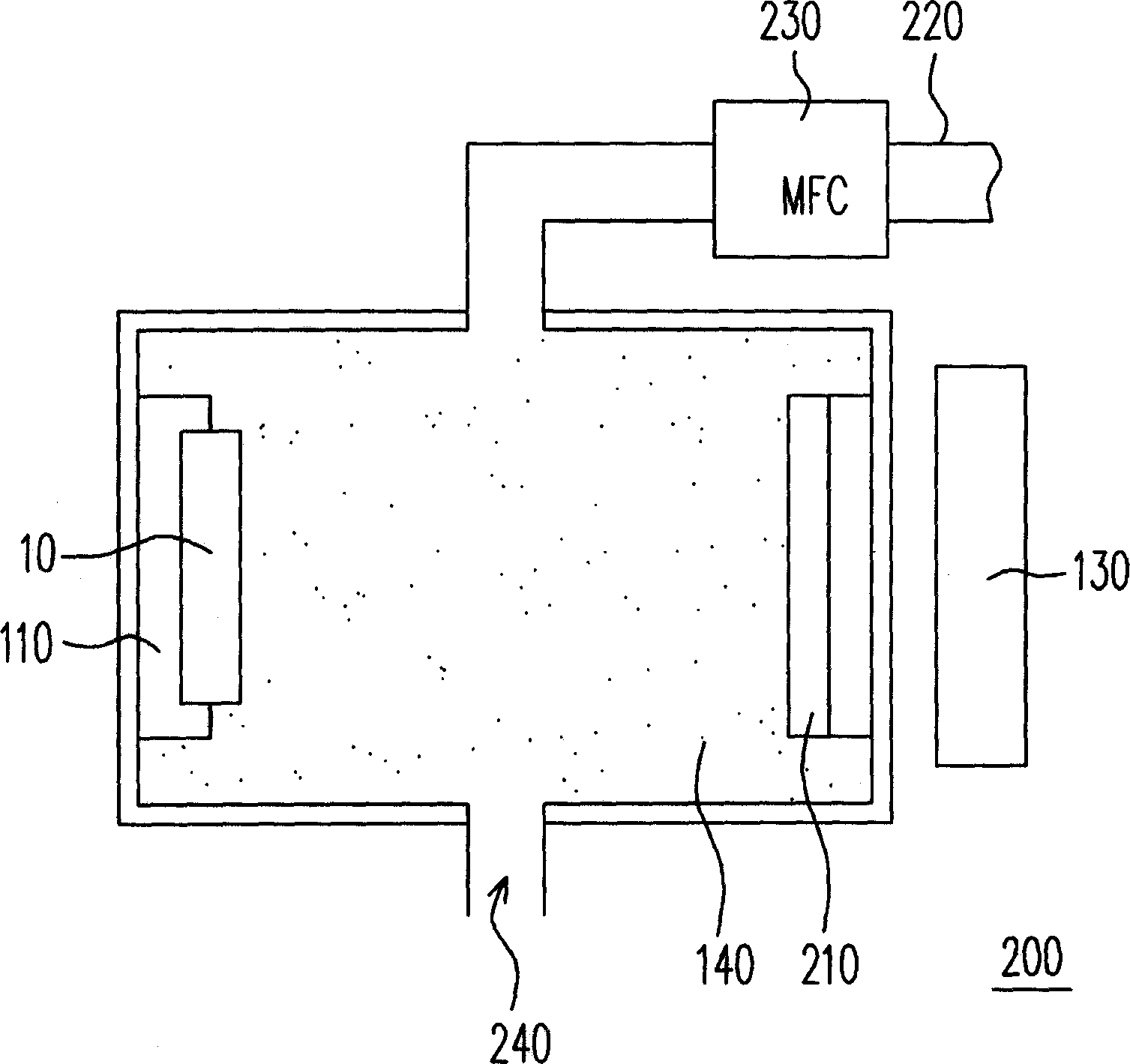
[0015] Figure 3A It is a schematic diagram of a reaction chamber used in a magnetron sputtering manufacturing process of a preferred embodiment of the present invention. Please refer to Figure 3A , The magnetron sputtering manufacturing process of this embodiment includes the following steps. Firstly, a reaction chamber 200 (reaction chamber) is firstly provided. The reaction chamber 200 at least includes a substrate base 110, a target 210, a magnetron device 130, and a process gas 140. The material of the target 210 is, for example, aluminum or an aluminum alloy. Or it is a metal whose melting point is higher than that of aluminum or aluminum alloy, such as metals such as chromium, molybdenum, tungsten, titanium or tantalum or alloys thereof. The substrate holder 110 can fix the substrate 10 in the reaction chamber 200 and can heat the substrate 10 .

[0016] Please continue to refer to Figure 3A , the substrate holder 110 and the target material 210 are arranged in th...


PUM


Abstract

The magnetically controlled sputtering process includes the following steps: the first providing a reaction chamber with at least base board seat, target material of aluminum, aluminum alloy or other metal of smelting point higher than that of aluminum or aluminum alloy, and magnetic controller; the subsequent transferring the base board onto the base board seat; and regulating the pressure inside the reaction chamber to 0.1-0.35 pa and sputtering to deposit film on the base board continuously. The process has high film quality.

Description

technical field [0001] The present invention relates to a thin film deposition manufacturing process, and in particular to a magnetron sputtering manufacturing process (magnetron sputtering process). Background technique [0002] In general semiconductor and flat panel display (Flat Panel Display, FPD) substrate thin film deposition manufacturing process can be roughly divided into physical vapor deposition manufacturing process and chemical vapor deposition manufacturing process. As far as the physical vapor deposition manufacturing process is concerned, the common sputtering manufacturing process works as follows: by applying an electric field, the ions in the chamber hit the metal target, and at this time the surface of the metal target is bombarded by the ions. Many secondary electrons (secondary electrons) and metal target atoms are generated. [0003] Then, the secondary electrons have obtained enough energy through the electric field to collide with the gas molecules...

Claims


Application Information

Patent Timeline
IPC IPC(8): C23C14/35
Inventor 李育舟锺享显许泓译
Owner CHUNGHWA PICTURE TUBES LTD
Why Eureka
Try Eureka