Panel display with anti secondary electron emission supporting wall structure and its making process
A secondary electron emission, flat panel display technology, used in the manufacture of discharge tubes/lamps, cathode ray/electron beam tube shells/containers, electrode systems, etc. Scrap and other problems, to prevent secondary electron emission and improve the success rate of production
- Summary
- Abstract
- Description
- Claims
- Application Information
AI Technical Summary
Problems solved by technology
Method used
Image
Examples
Embodiment Construction
[0041] The present invention will be further described below in conjunction with the accompanying drawings and embodiments, but the present invention is not limited to these embodiments.
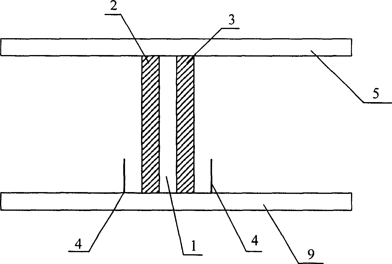
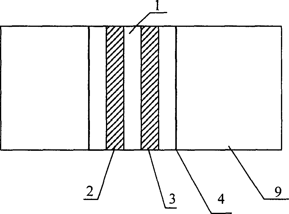
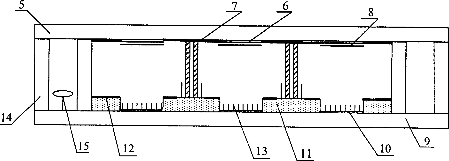
[0042] The present invention includes a sealed vacuum chamber composed of an anode glass panel 5, a cathode glass panel 9 and a surrounding glass frame 14. An anode conductive strip 6 and a phosphor layer printed on the anode conductive strip 6 are arranged on the anode glass panel 5. 8. On the cathode panel 9, a cathode conductive strip 10, an insulating spacer layer 11, a printed carbon nanotube cathode 13, a control grid strip 12 for controlling electron emission, and an auxiliary getter element 15 are arranged in a sealed vacuum chamber A support wall structure is provided which can not only provide support for the glass panel, but also prevent secondary electron emission on the support wall structure.
[0043] The support wall structure for preventing secondary electron emission compris...
PUM
 Abstract
Description
Claims
Application Information
 - R&D
- Intellectual Property
- Life Sciences
- Materials
- Tech Scout
- Unparalleled Data Quality
- Higher Quality Content
- 60% Fewer Hallucinations
Browse by: Latest US Patents, China's latest patents, Technical Efficacy Thesaurus, Application Domain, Technology Topic, Popular Technical Reports.
© 2025 PatSnap. All rights reserved.Legal|Privacy policy|Modern Slavery Act Transparency Statement|Sitemap|About US| Contact US: help@patsnap.com


