Transistor and method of manufacturing the same
A transistor and crystal structure technology, applied in semiconductor/solid-state device manufacturing, semiconductor devices, electrical components, etc., can solve the problems of steep PN junction, cannot be easily applied, low resistance, etc., to prevent short-channel effect, improve electrical Effects of Features
- Summary
- Abstract
- Description
- Claims
- Application Information
AI Technical Summary
Problems solved by technology
Method used
Image

Examples
Embodiment 1
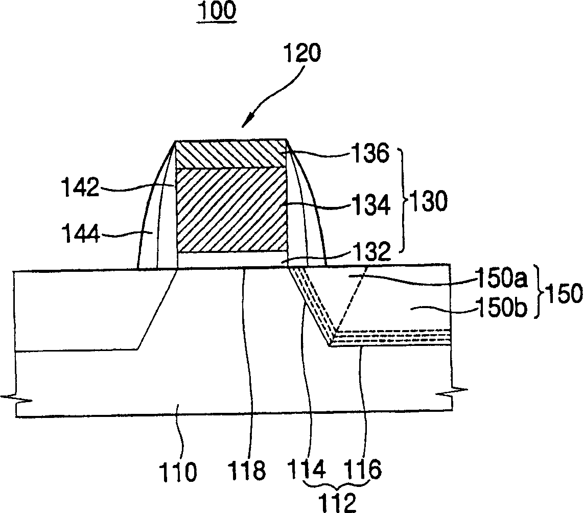
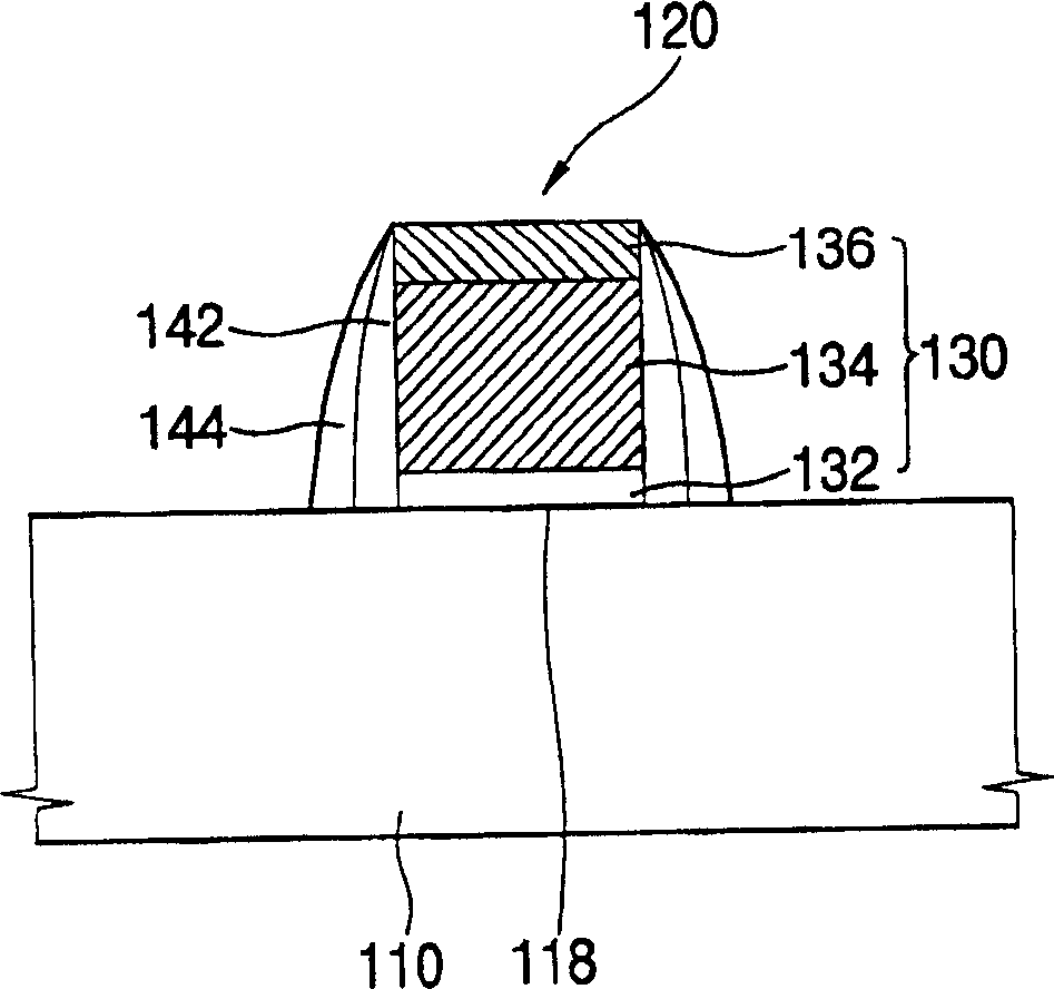
[0054] figure 1 is a cross-sectional view showing a transistor according to a first embodiment of the present invention.
[0055] refer to figure 1 , the transistor 100 of this embodiment includes a semiconductor substrate 110 such as a silicon (Si) substrate or a silicon-germanium (Si-Ge) substrate, a gate structure 120 formed on the semiconductor substrate 110 , a gate structure 120 formed on the semiconductor substrate 110 The two epitaxial layers 150 adjacent to the gate structure 120 and the impurity regions respectively formed in the epitaxial layers 150 .
[0056] The semiconductor substrate 110 has a surface 118 including silicon oriented in the {100} plane. Gate structure 120 is formed on surface 118 of substrate 110 .
[0057] Two recesses 112 are respectively formed at portions of the surface 118 adjacent to the gate structure 120 . Recess 112 includes a bottom surface 116 and side surfaces 114, respectively. Bottom surface 116 includes silicon oriented in a {1...
Embodiment 2
[0078] Such as Figure 7 As shown, the transistor of the second embodiment of the present invention has the same figure 1 The elements of the transistor are substantially the same, except for the impurity region 170 having a side surface quite different from that of the epitaxial layer 150 . The side surfaces of the impurity region 170 are located between the central portion of the gate pattern 130 and the side surfaces of the epitaxial layer 150, respectively. Therefore, any other detailed descriptions about the transistors of this embodiment will not be repeated.
[0079] Image 6 with 7 is a cross-sectional view showing a method of manufacturing the transistor according to the present embodiment. In this embodiment, the process of manufacturing the transistor is basically the same as the reference Figures 2 to 5 The same as described except for the process of forming impurity region 170 .
[0080] refer to Image 6 Impurities including carbon, boron, phosphorus, etc...
Embodiment 3
[0084] The transistor of the third embodiment of the present invention has the same figure 1 The transistors are basically the same structure. Therefore, will refer to Figures 8 to 12 A method of manufacturing the transistor of this embodiment is described.
[0085] Figures 8 to 12 is a cross-sectional view showing a method of manufacturing a transistor according to a third embodiment of the present invention. In this embodiment, the epitaxial layer 150 is formed in the recess 112 after the first spacer 142 is formed on the sidewall of the gate pattern 130 and before the second spacer 144 is formed on the first spacer 142 .
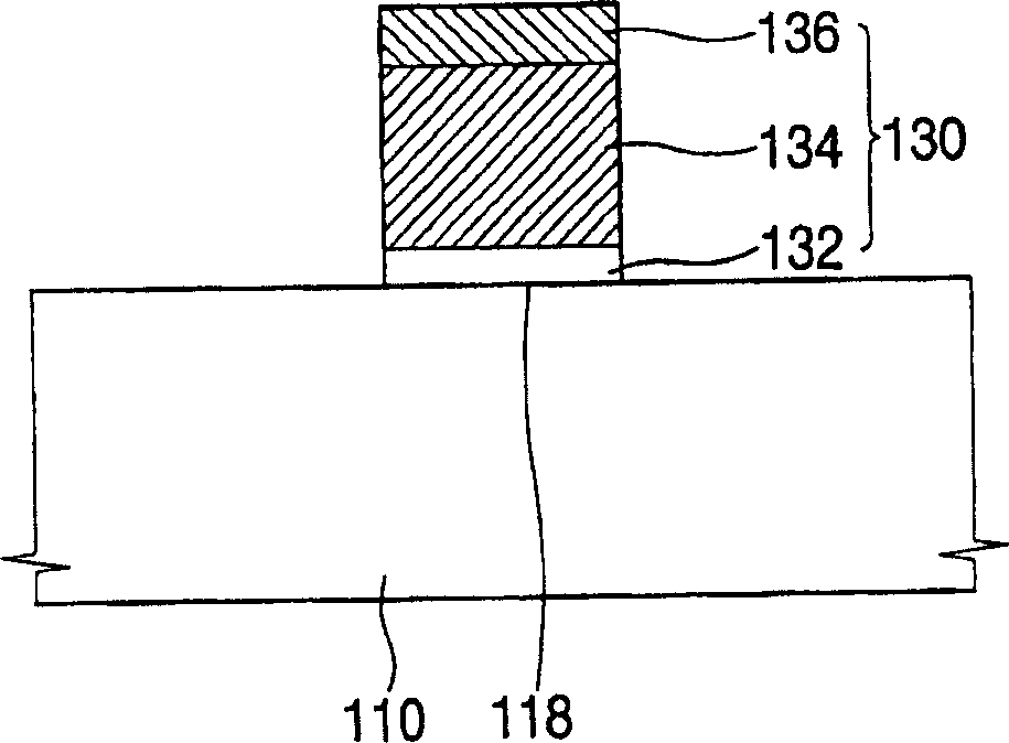
[0086] refer to Figure 8 , a gate pattern 130 including an insulating layer pattern 132 , a conductive layer pattern 134 and a hard mask layer pattern 136 is formed on the surface 118 of the semiconductor substrate 110 . Surface 118 includes silicon oriented in the {100} plane.
[0087] refer to Figure 9 , forming first spacers 142 including ni...
PUM
 Abstract
Description
Claims
Application Information
 - R&D
- Intellectual Property
- Life Sciences
- Materials
- Tech Scout
- Unparalleled Data Quality
- Higher Quality Content
- 60% Fewer Hallucinations
Browse by: Latest US Patents, China's latest patents, Technical Efficacy Thesaurus, Application Domain, Technology Topic, Popular Technical Reports.
© 2025 PatSnap. All rights reserved.Legal|Privacy policy|Modern Slavery Act Transparency Statement|Sitemap|About US| Contact US: help@patsnap.com