Semiconductor laser assembly
A technology of laser diodes and heat sinks, applied in lasers, laser parts, semiconductor lasers, etc., can solve problems such as unfavorable laser characteristics and effects, and achieve the effect of improving contact performance
- Summary
- Abstract
- Description
- Claims
- Application Information
AI Technical Summary
Problems solved by technology
Method used
Image
Examples
no. 1 example
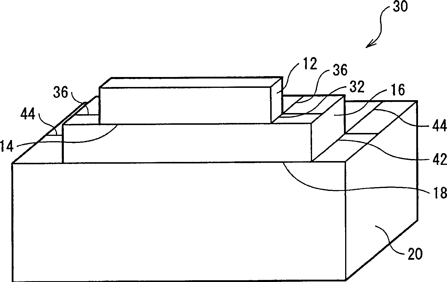
[0113] This embodiment is an example of the laser diode device according to the first invention.
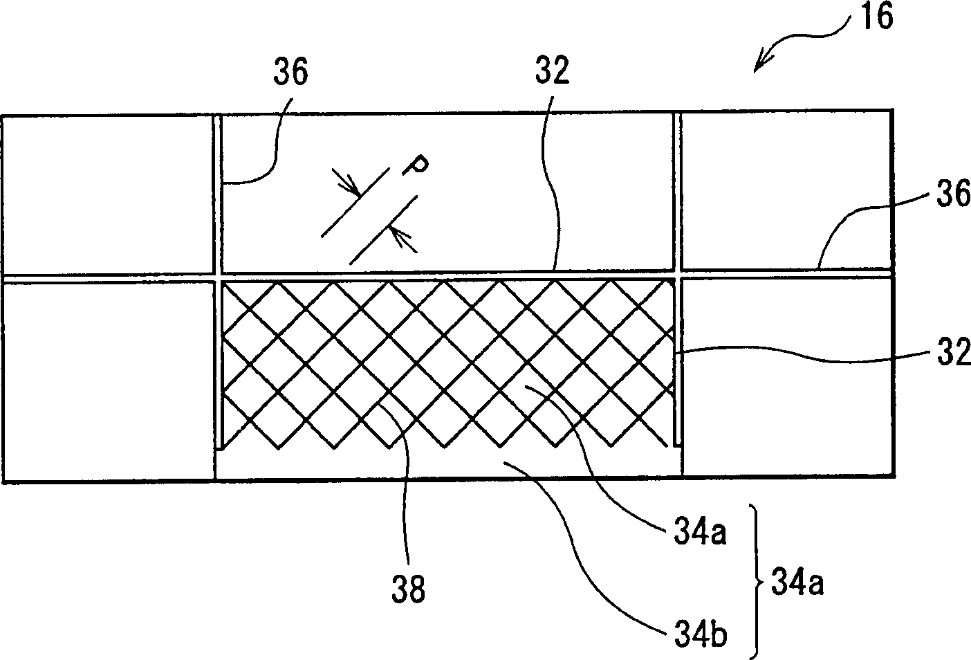
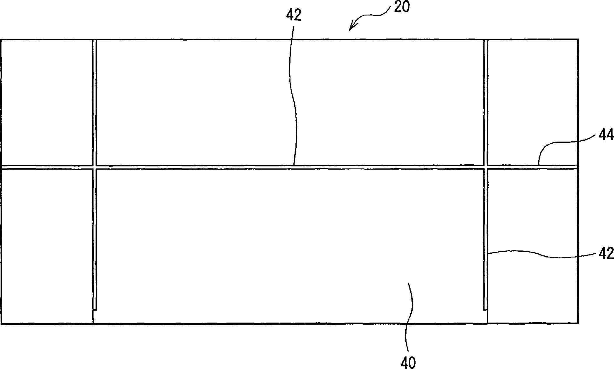
[0114] figure 1 Shown is the structure of most parts of the laser diode device, figure 2 Shown is the structure of the abutment groove, image 3 Shown is the structure of the radiator slot.
[0115] Such as figure 1 As shown, as most of the parts similar to the conventional laser device 10, the laser diode device 30 of the present embodiment includes: a laser diode device 12, a base 16 welded to the substrate side of the laser diode device 12, and a second pedestal between the two A solder layer 14; a heat sink 20 soldered to the back side of the submount 16 with a second solder layer 18 in between.
[0116] In the laser diode device 30 , the submount 16 includes a groove 32 (hereinafter referred to as a submount groove) and an extension groove 36 . An abutment groove 32 is formed around the welding region 34 along the edge of the welding region 34 to which the laser diod...
no. 2 example
[0137] This embodiment relates to a laser diode device according to the second invention. Figure 5 Shown is the structure of most parts of the laser diode device 50, and Image 6 Shown is the structure of the radiator slot.
[0138] The structure of the laser diode device 50 is the same as that of a conventional laser device 10 except that the laser diode device 12 is soldered directly to the heat sink 20 without the submount 16 described above.
[0139] In the present embodiment, the heat sink 20 includes a groove 52 (hereinafter referred to as a heat sink groove) and an extension groove 56 . A heat sink groove 52 is formed around the soldering area 54 along the edge of the soldering area 54 to be soldered with the laser diode device 12 . The extension slot 56 extends from the radiator slot 52 to the radiator 20 .
[0140] A heat sink groove 52 is formed around the solder area 54 along the edge of the solder area 54 of the heat sink 20 on the rear surface side in the dire...
no. 3 example
[0150] This embodiment relates to a laser diode device according to the third invention. Figure 9 Shown is the structure of the abutment therein.
[0151] The structure of the laser diode device of this embodiment is the same as that of the laser diode device 30 of the first embodiment except for the structure of the base groove.
[0152] In this embodiment, the abutment 16 includes an abutment transverse groove 62 . This lateral groove 62 intersects with the center of the welding region 34 where the laser diode device 12 is welded in a direction parallel to the emitting end surface of the laser diode device 12 (refer to figure 1 ), and reach the edge of the abutment 16.
[0153] The size of the abutment lug groove 62 is the same as that of the abutment groove 32 in the first embodiment. There may be multiple abutment transverse grooves 62 . Still further, it is not essential that the abutment lug 62 intersects the central portion of the welding area 34 of the abutment 16 ...
PUM
 Abstract
Description
Claims
Application Information
 - R&D
- Intellectual Property
- Life Sciences
- Materials
- Tech Scout
- Unparalleled Data Quality
- Higher Quality Content
- 60% Fewer Hallucinations
Browse by: Latest US Patents, China's latest patents, Technical Efficacy Thesaurus, Application Domain, Technology Topic, Popular Technical Reports.
© 2025 PatSnap. All rights reserved.Legal|Privacy policy|Modern Slavery Act Transparency Statement|Sitemap|About US| Contact US: help@patsnap.com


