Process for preparing conductive polymer periodic microstructure
A conductive polymer and periodic technology, applied in the field of conductive polymers, can solve the problems of high device requirements and inability to form a periodic structure of conductive polymers at one time
- Summary
- Abstract
- Description
- Claims
- Application Information
AI Technical Summary
Problems solved by technology
Method used
Image
Examples
Embodiment 1
[0021] ① Prepare a conductive polymer film on the surface of the substrate; take 0.2ml aniline and 360mg silver nitrate and dissolve them in DMF (N,N'-dimethylformamide), then mix the above two solutions and immerse a glass substrate material in the solution Inside, the glass substrate was taken out after three hours, and a thin film was formed on its surface, which was rinsed with ethanol and dried under a nitrogen atmosphere to form a thin film glass sample, which was placed on the sample stage.
[0022] ②Formation of femtosecond laser coherent field: select a femtosecond pulse with a pulse width of 120fs, a wavelength of 800nm, a pulse repetition rate of 6Hz, and a pulse energy of 70μJ. The femtosecond pulse beam is divided into two beams by a beam splitter, and the beam diameter is 6mm, the angle between the two beams is 40°, use two focusing lenses with a focal length of 10cm to focus the two beams on the surface of the film, form a femtosecond laser coherent field, irradi...
Embodiment 2
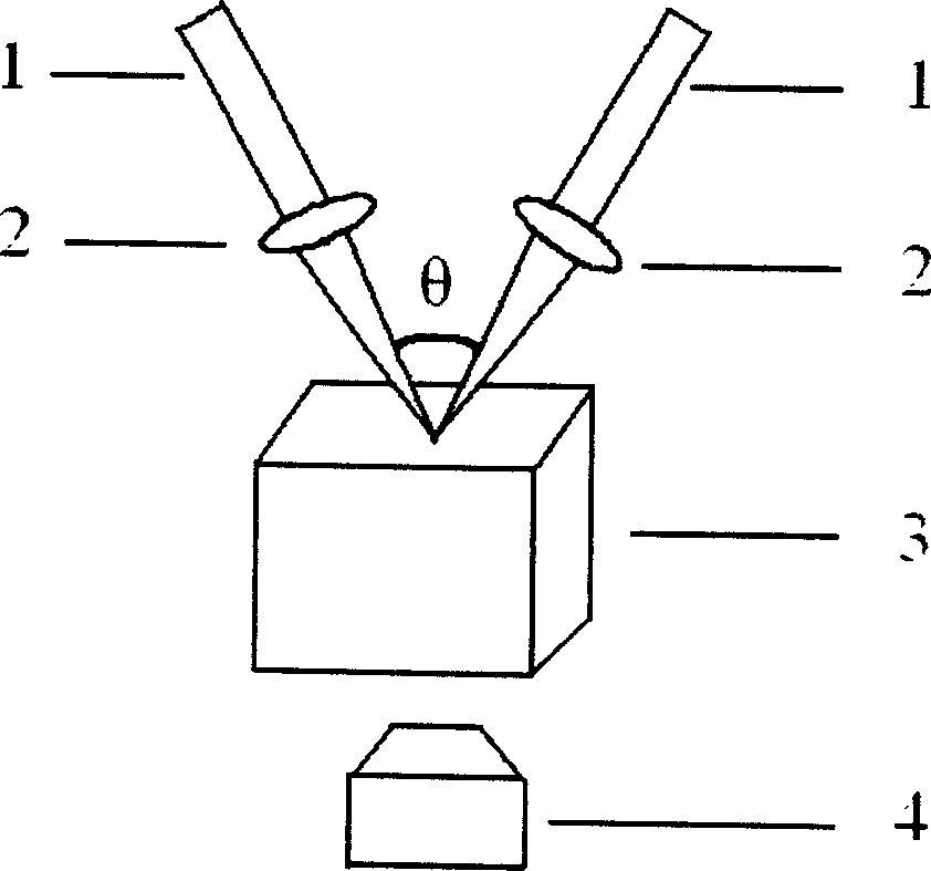
[0026] Take 0.2ml of aniline and 360mg of silver nitrate and dissolve them in DMF (N,N'-dimethylformamide), then mix the above two solutions and immerse a glass matrix material into the solution, take out the glass matrix after three hours, and then A thin film was formed on the surface, which was rinsed with ethanol and dried under a nitrogen atmosphere. The above film was placed on the sample stage. Select a femtosecond pulse with a pulse width of 120fs, a wavelength of 800nm, a pulse repetition rate of 6Hz, and a pulse energy of 70μJ. The beam is divided into two beams by a beam splitter, the beam diameter is 6mm, and the angle between the two beams is 40°. The sample is controlled by a computer-operated three-dimensional mobile platform, and the structure of the experimental device is as follows: figure 1 . Use two focusing lenses with a focal length of 10cm to focus the two light beams on the surface of the film and control the movement of the sample stage, so that a se...
Embodiment 3
[0028] Set up an electrochemical three-electrode reaction system, working electrode: ITO conductive glass, reference electrode: silver / silver chloride, counter electrode: platinum sheet. The solution uses 0.5mol / L pyrrole + 1mol / L LiClO 4 Polypropylene carbonate solution. A conductive polymer film was prepared on the ITO conductive glass by using the potentiodynamic deposition method to cycle for one cycle in the range of 0-0.8V. The polypyrrole film was cleaned with polypropylene carbonate and blown dry with nitrogen. The above film was placed on the sample stage. Select a femtosecond pulse with a pulse width of 120fs, a wavelength of 800nm, a pulse repetition rate of 1Hz, and a pulse energy of 70μJ. The beam is divided into two beams by a beam splitter, the beam diameter is 6mm, and the angle between the two beams is 70°. The sample is controlled by a computer-operated three-dimensional mobile platform, and the structure of the experimental device is as follows: figure 1...
PUM
| Property | Measurement | Unit |
|---|---|---|
| diameter | aaaaa | aaaaa |
Abstract
Description
Claims
Application Information
 - R&D
- Intellectual Property
- Life Sciences
- Materials
- Tech Scout
- Unparalleled Data Quality
- Higher Quality Content
- 60% Fewer Hallucinations
Browse by: Latest US Patents, China's latest patents, Technical Efficacy Thesaurus, Application Domain, Technology Topic, Popular Technical Reports.
© 2025 PatSnap. All rights reserved.Legal|Privacy policy|Modern Slavery Act Transparency Statement|Sitemap|About US| Contact US: help@patsnap.com


