Testing method for chip synchronous clock and chip capable of synchronously testing clock function

A technology of synchronous clock and synchronous testing, applied in the direction of semiconductor/solid-state device testing/measurement, etc., can solve the problems of affecting the test results, difficulty in chip design, and inability to cross the delay time.

Active Publication Date: 2005-06-29
VIA TECH INC
View PDF0 Cites 0 Cited by
  • Summary
  • Abstract
  • Description
  • Claims
  • Application Information

AI Technical Summary

Problems solved by technology

However, when performing chip testing, since the output signal of the chip must be compared with the ideal signal, and when the output signal is completely consistent with the ideal signal, the manufacturing quality of the chip can be confirmed to be flawless. Therefore, the sampling caused by the asynchronous effect Errors will affect the test results
[0009] It can be seen from the above that in order to avoid the asynchronous effect from affecting the chip test results, the delay time of the logic circuit Lg cannot exceed 1ns (0.8ns~1.2ns), 2ns (1.7~3.2ns) and 3ns (2.8ns~3.2ns). Therefore, In the design of the flip-flop logic circuit, the delay time of the logic circuit Lg must be limited, which leads to difficulties in chip design

Method used


Image

  • Testing method for chip synchronous clock and chip capable of synchronously testing clock function
  • Testing method for chip synchronous clock and chip capable of synchronously testing clock function
  • Testing method for chip synchronous clock and chip capable of synchronously testing clock function

Examples


Embodiment Construction

[0022] The invention provides a chip testing method, which can avoid problems caused by asynchronous effects and improve the accuracy of chip testing.

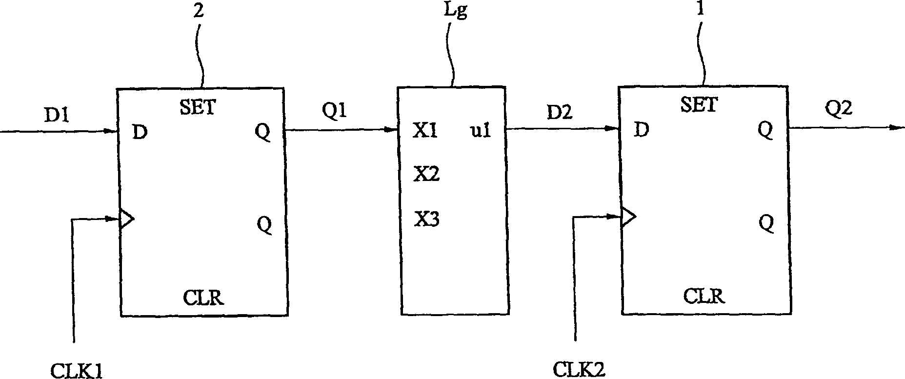
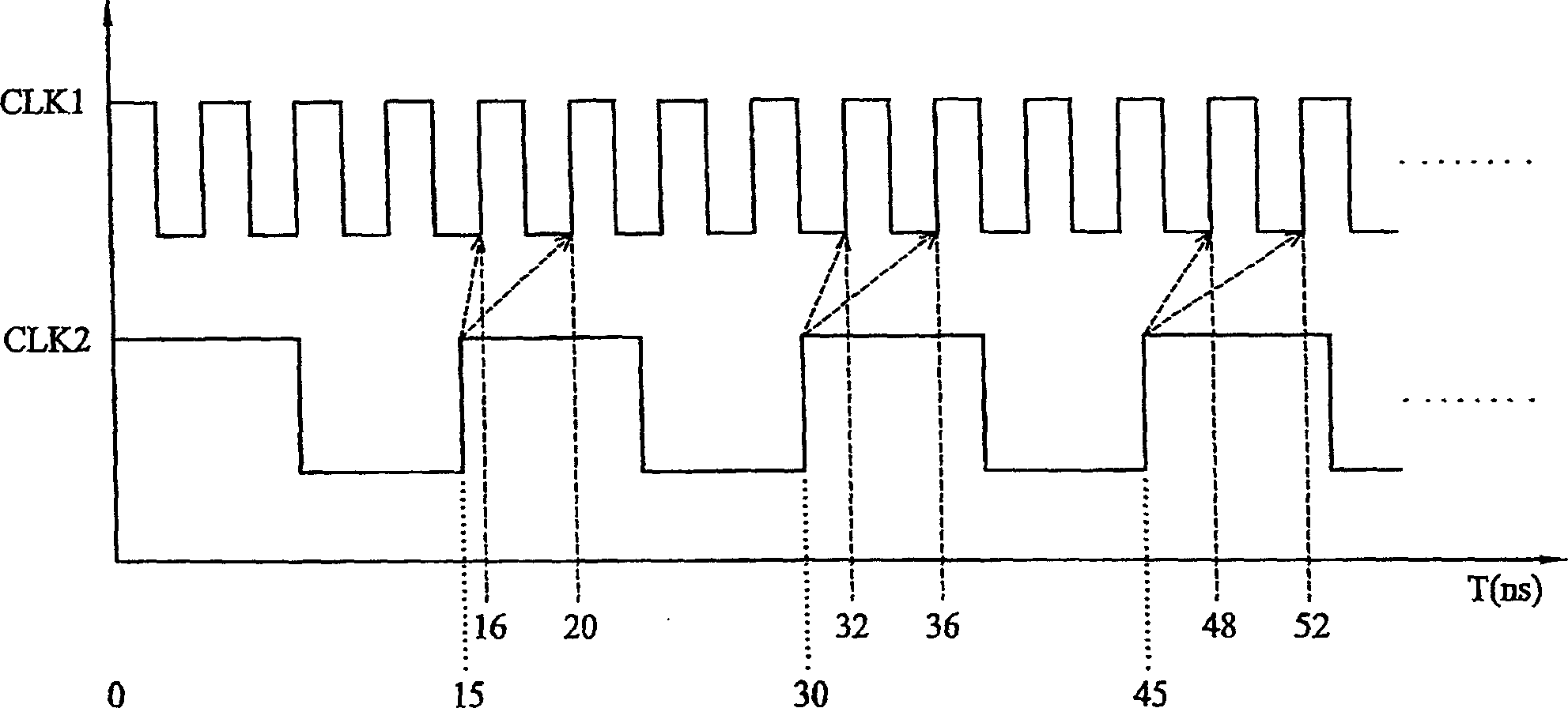
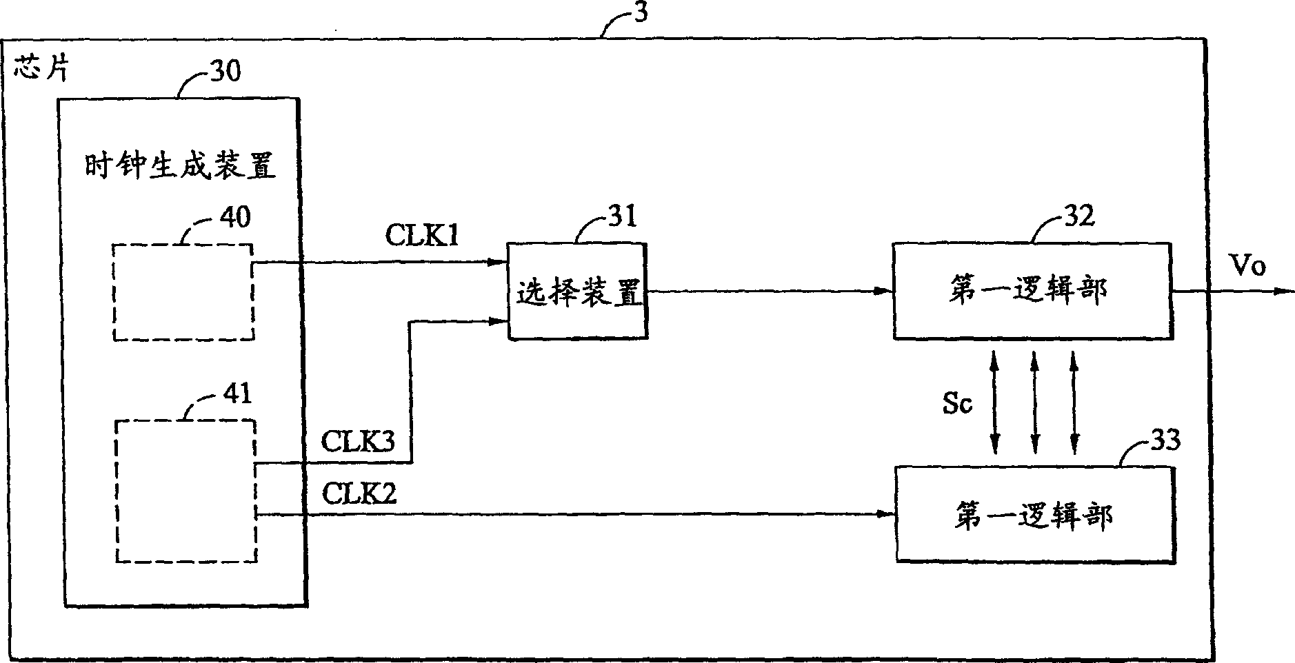
[0023] image 3 A chip to which the chip testing method of the present invention is applied is shown. Wherein, the chip 3 includes a clock generating device 30 , a selecting device 31 , a first logic part 32 and a second logic part 33 . During normal operation, the first logic part 32 is driven by the first clock signal CLK1, the second logic part 33 is driven by the second clock signal CLK2, and the operating frequency of the first clock CLK1 is higher than that of the second clock CLK2 and is not Integer multiples of the working frequency of the second clock signal CLK2. The clock generating device 30 includes a first clock generating device 40 and a second clock generating device 41; the first clock generating device 40 is used to generate the first clock signal CLK1, and the second clock generating device 41 is used to g...


PUM


Abstract

It is a chip with clock test function and its test method. The above chip at least comprises one first logic part, one-second logic part. The method comprises the following steps: to generate one third clock signal; to substitute the first clock signal with third clock signal; to test the above the part outside the first clock generation device of the chip; to make the first logic operation independent to the second logic part to test the first clock generation device.

Description

technical field [0001] The invention relates to a chip testing method, in particular to a chip testing method capable of avoiding sampling errors produced by asynchronous effects. Background technique [0002] Generally, in the chip manufacturing process, the chip testing process must be passed at the end to confirm the manufacturing quality of the chip. In the process of chip testing, the computer simulates the ideal output signal of the chip at a specific input signal and records it; then, the same specific input signal is provided to the chip to be tested, and then the output signal of the chip under test is compared with the The ideal output signal is compared to determine whether it is consistent, and to determine whether there is a defect in the chip manufacturing process. [0003] In order to meet different requirements of electronic products, the operating frequencies required by each chip specification are different, for example, chips with two different operating ...

Claims


Application Information

Patent Timeline
IPC IPC(8): H01L21/66
Inventor 谢易霖
Owner VIA TECH INC
Why Eureka
Try Eureka