Resonant tunneling micro mechanical force sensor and method for manufacturing the same
A resonant tunneling and force sensor technology, which is applied in the field of micro-electromechanical systems and sensing, can solve the problems of limiting the working range of the sensor, difficult to maintain, and low yield, and achieves a technology suitable for mass production, small temperature coefficient, and low power. consumption effect
- Summary
- Abstract
- Description
- Claims
- Application Information
AI Technical Summary
Problems solved by technology
Method used
Image
Examples
Embodiment 1
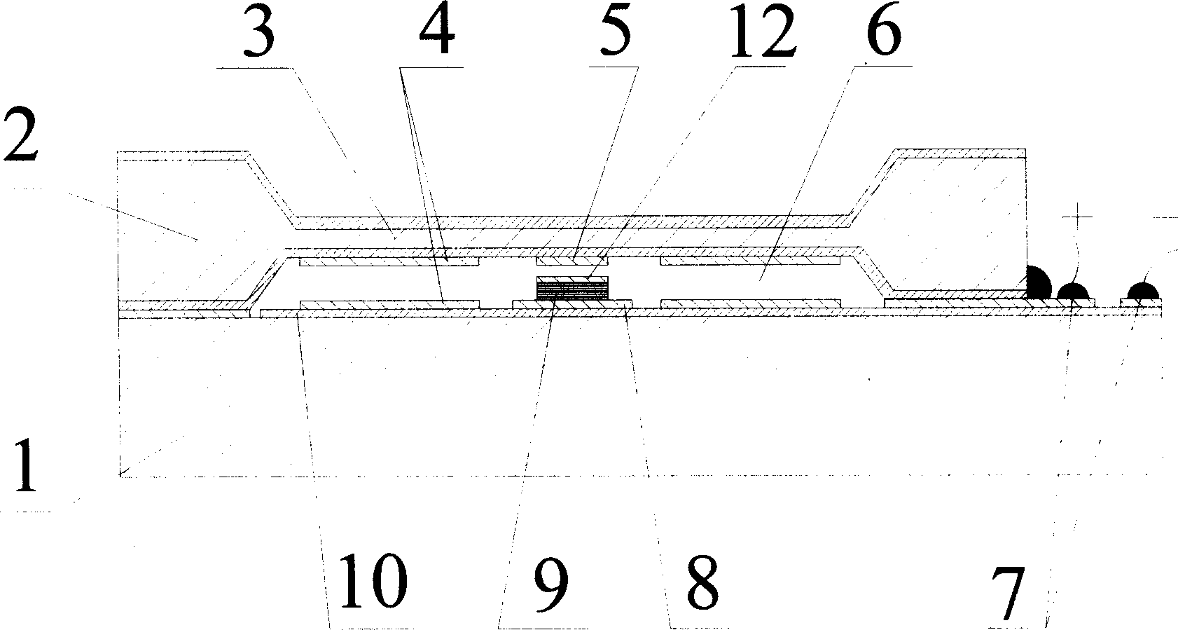
[0018] Such as figure 1 Shown is an embodiment of the resonant tunneling micromechanical force sensor, that is, a structural schematic diagram of a micromechanical pressure sensor. The main structure of the resonant tunneling micromechanical pressure sensor is composed of two parts: an upper silicon wafer 1 and a lower silicon wafer 2. The sheet 2 includes a lower driving electrode 4 grown on its upper surface, a tunnel cathode 8 grown on its upper surface corresponding to the tunnel anode 5 , and a multi-thin layer structure grown on the surface of the tunnel cathode 8 . The tunneling junction 9 has a control electrode 12 grown on the surface of the tunneling junction 9 to control the emission of tunneling electrons. When working, a certain voltage is first applied between the upper and lower driving electrodes 4, and the electrostatic attraction between the two electrodes is controlled by feedback to keep the gap between the tunneling anode 5 and the control electrode 12 at...
Embodiment 2
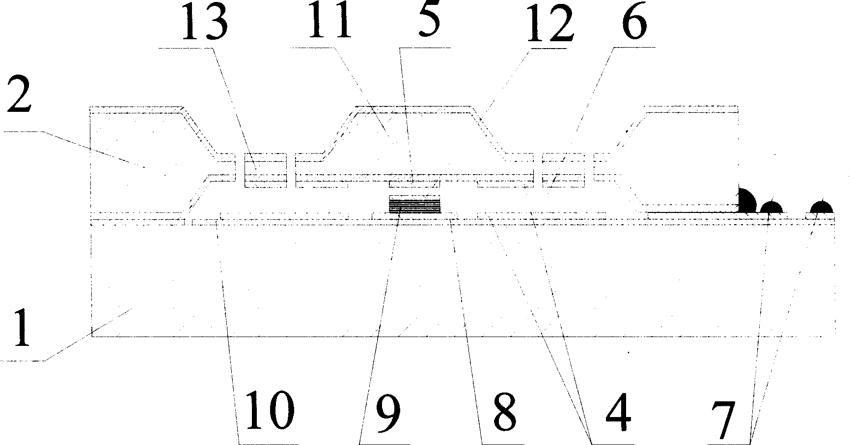
[0045] Such as figure 2 Shown is a schematic diagram of the structure of a resonant tunneling micromachined accelerometer. The main structure of the resonant tunneling micromachined accelerometer consists of two parts: an upper silicon wafer 1 and a lower silicon wafer 2. The upper silicon wafer 1 includes a silicon beam 13 and a silicon island 11 on it, and the lower surface of the silicon beam 13 and the silicon island 11. The grown upper drive electrode 4 and the tunnel anode 5, the lower silicon chip 2 includes the lower drive electrode 4 grown on its upper surface, and also includes the tunnel cathode 8 grown on its upper surface corresponding to the tunnel anode 5, and A tunneling junction 9 with a multi-thin layer structure is grown on the surface of the tunneling cathode 8 , and a control electrode 12 for controlling the emission of tunneling electrons is grown on the surface of the tunneling junction 9 . When working, a certain voltage is first applied between the u...
PUM
 Abstract
Description
Claims
Application Information
 - Generate Ideas
- Intellectual Property
- Life Sciences
- Materials
- Tech Scout
- Unparalleled Data Quality
- Higher Quality Content
- 60% Fewer Hallucinations
Browse by: Latest US Patents, China's latest patents, Technical Efficacy Thesaurus, Application Domain, Technology Topic, Popular Technical Reports.
© 2025 PatSnap. All rights reserved.Legal|Privacy policy|Modern Slavery Act Transparency Statement|Sitemap|About US| Contact US: help@patsnap.com


