High-resolution digital pulse width modulator and method for generating a high-resolution pulse width modulated signal

A technology of pulse width modulation and high resolution, applied in the direction of pulse generation, electric pulse generation, pulse duration/width modulation, etc., can solve the problems of unfavorable high clock frequency and interference

Inactive Publication Date: 2005-06-01
INFINEON TECH AG
View PDF4 Cites 12 Cited by
  • Summary
  • Abstract
  • Description
  • Claims
  • Application Information

AI Technical Summary

Problems solved by technology

[0010] However, the fixed design of the flip-flops, or delay stages, as well as the generation of the clock signal in the pulse width modulators themselves, makes it difficult to communicate with an external clock signal when there is exactly one system clock. In addition, the delay time of each delay stage, and thus the system clock, will depend on fluctuations in the supply voltage in the operating temperature, or on transistor parameters during production , which can lead to mixed frequency products in adjacent telecommunication circuit parts, for example, in mobile circuits used in a plurality of frequency bands (dual-band or triple-band circuits), and in addition, in demodulation After the change, these mixed frequency products will produce noise that interferes with the sound in the useful signal (for example, in a voice signal), and in the digital control loop, a low system clock rate will produce A larger phase rotation (phaserotation) of the transfer function of the control loop, and therefore, a smaller phase edge of the control loop, which reduces attenuation and may thus cause unwanted natural Oscillation, however, in circuit configurations based on known technology, high clock frequencies can only be achieved less favorably by hardware changes or new developments, therefore, a device for pulse width modulation is required, and the The device will operate in a stable manner at high and variable (external) clock frequencies

Method used


Image

  • High-resolution digital pulse width modulator and method for generating a high-resolution pulse width modulated signal
  • High-resolution digital pulse width modulator and method for generating a high-resolution pulse width modulated signal
  • High-resolution digital pulse width modulator and method for generating a high-resolution pulse width modulated signal

Examples


Embodiment Construction

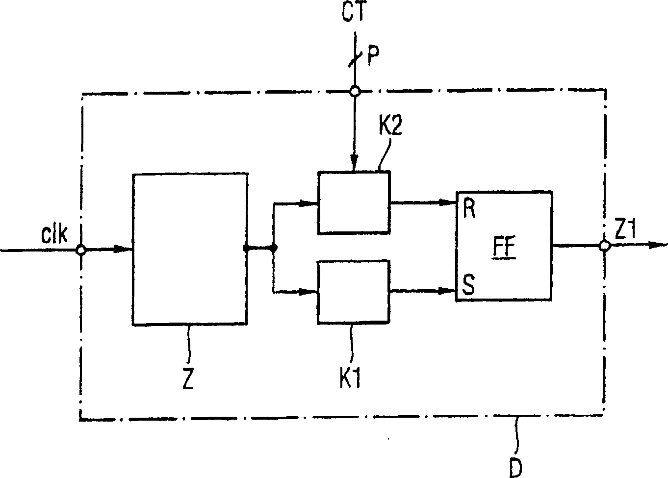
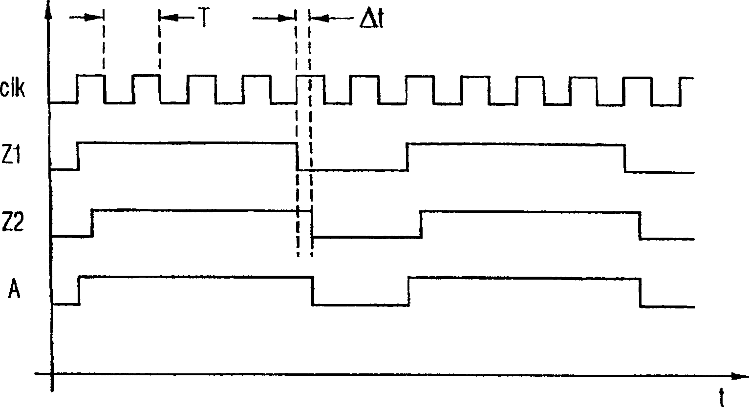
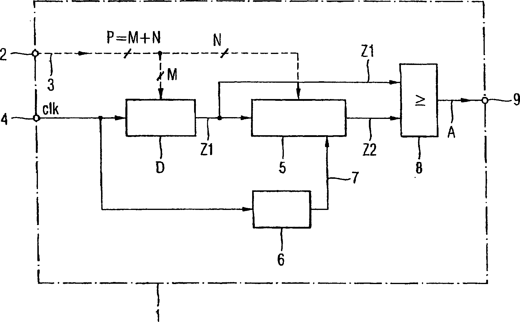
[0034] Figure 2 shows a clock signal clk having a clock period T and a first pulse width modulated intermediate signal Z1, and wherein the pulse width of the first pulse width modulated intermediate signal is the clock period T a multiple. According to the invention, the first intermediate signal Z1 is provided by a pulse width modulator unit D on the basis of known techniques, and the second intermediate signal Z2 is generated from (already by a delay The first intermediate signal Z1 delayed by a time Δt, in this particular example, the clock signal clk is utilized in such a way that the delay time Δt is exactly a quarter of the clock period T. To control the delay time Δt, in addition, for example, logically combining the two intermediate signals Z1 and Z2 by means of a logical OR function will generate an output signal A which will have the same value as the first A rising edge of the rising edge of the intermediate signal Z1, and a falling edge of the output signal A wil...


PUM


Abstract

A high-resolution digital pulse width modulator having a digital pulse width modulator unit for receiving a clock signal and for receiving the first bit of a digital control signal to generate a pulse width of the clock A pulse width modulated first pulse width modulated intermediate signal of an integer multiple of the period also has a programmable signal delay path for use based on the second bit of the digital control signal by delaying the first intermediate signal by a programmable delay time for outputting at least one pulse width modulated intermediate signal, the signal delay time being synchronized with the clock signal, and having a logic circuit for The intermediate signals are logically combined and output to form a pulse width modulated signal.

Description

technical field [0001] The present invention relates to a high resolution digital pulse width modulator and also to a method of generating a high resolution pulse width modulated signal. Background technique [0002] A pulse width modulator is used to drive a DC power supply and provide an on time and an off time in a specific switching cycle, and pulse width modulation is by changing the ratio of the on time to the off time To be realized, when driving a DC power supply, an extended turn-on time will provide a larger arithmetic mean value for the output voltage and, therefore, provide a larger output current. In addition, the pulse width modulated signal system It can also be used for information transmission, or to form an engine controller in automotive technology. [0003] In a similar design, a pulse width modulated signal can be generated by comparing a triangular wave voltage at a fixed frequency with a variable DC control voltage if the control voltage is greater th...

Claims


Application Information

Patent Timeline
IPC IPC(8): H03K3/017H03K7/08
CPCH03K7/08
Inventor A·斯泰斯查登
Owner INFINEON TECH AG
Why Eureka
Try Eureka