
Adhesive sheet for semiconductor device manufacture, semiconductor device using it and manufacturing method

A technology for semiconductors and adhesive sheets, which is used in the manufacture of semiconductor/solid-state devices, semiconductor devices, and electrical solid-state devices, and can solve problems such as unqualified connections.

Active Publication Date: 2005-06-01
TOMOEGAWA PAPER CO LTD
View PDF1 Cites 6 Cited by
  • Summary
  • Abstract
  • Description
  • Claims
  • Application Information

AI Technical Summary

Problems solved by technology

In the case where such adhesive residue occurs, there is a concern that connection failure may occur when the manufactured semiconductor device is packaged on the wiring board due to the adhesion of the adhesive to the external connection terminal portion of the casting resin and the lead wires in the vicinity.

Method used

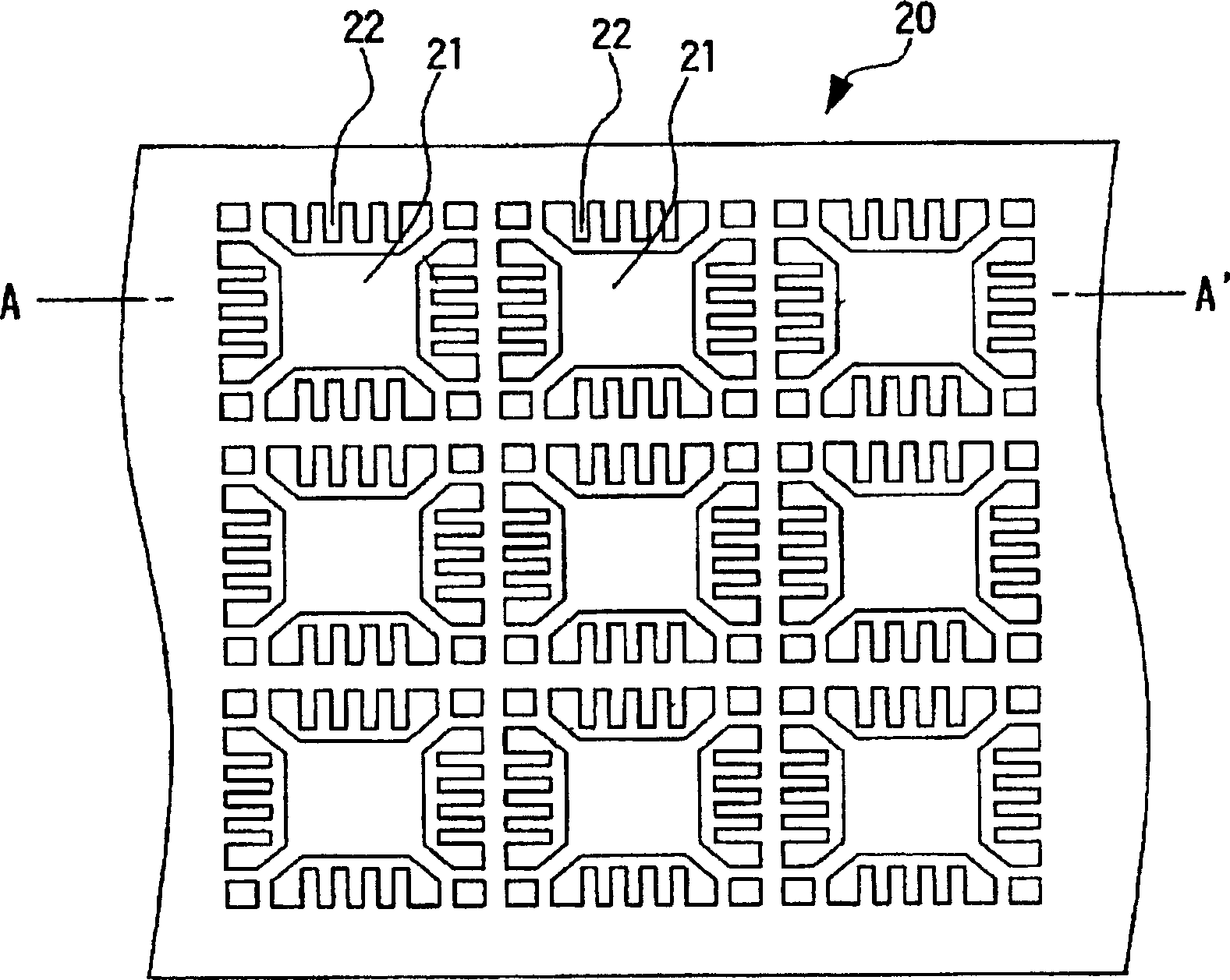
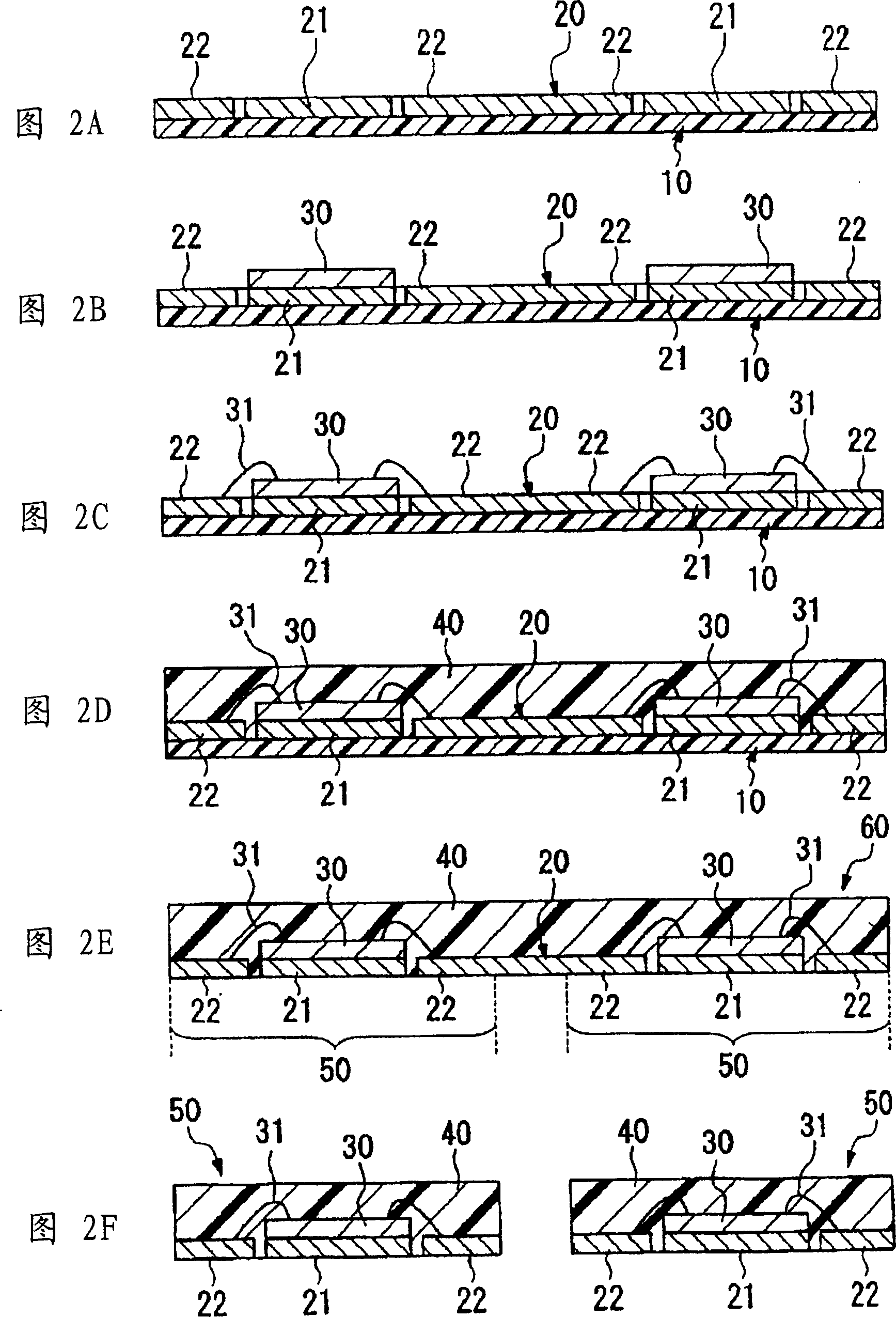

Image

  • Adhesive sheet for semiconductor device manufacture, semiconductor device using it and manufacturing method
  • Adhesive sheet for semiconductor device manufacture, semiconductor device using it and manufacturing method

Examples


Embodiment 1

[0070] With the compositions and compounding ratios shown in Table 1, adhesive solutions mixed with tetrahydrofuran were produced. Then, a polyimide resin film (manufactured by Toray Dupon Corporation, trade name: Capton 100EN, thickness 25 μm, glass transition temperature 300°C or above, thermal expansion coefficient 16ppm / °C) was used as the heat-resistant base material, And after coating the above-mentioned adhesive solution thereon, it dried at 120 degreeC for 5 minutes, and the thickness after drying was 6 micrometers, and the adhesive sheet of this invention which has an adhesive layer was obtained.

[0071] Furthermore, the weight ratio of the thermosetting resin component (a) to the thermoplastic resin component (b) is 1.5, and the ratio of (thermosetting resin component (a)+thermoplastic resin component (b)) / (removable component (c)) The weight ratio is 28.57.

Embodiment 2

[0073] The adhesive sheet of the present invention was obtained in the same manner as in Example 1 except that the adhesive solution was changed to the composition and compounding ratio shown in Table 1.

[0074] Furthermore, the weight ratio of the thermosetting resin component (a) to the thermoplastic resin component (b) is 1.5, and the ratio of (thermosetting resin component (a)+thermoplastic resin component (b)) / (removable component (c)) The weight ratio is 33.33.

Embodiment 3

[0076] The thermosetting resin component (a), the thermoplastic resin component (b) and the curing accelerator were mixed in tetrahydrofuran with the composition and compounding ratio shown in Table 1 to prepare an adhesive solution. Then, a polyimide resin film (manufactured by Toray Dupon Co., Ltd., trade name: ヵプトン 100EN, thickness 25 μm, glass transition temperature 300°C or above, thermal expansion coefficient 16ppm / °C) was used as the heat-resistant base material, After coating the above adhesive solution, dry it at 100°C for 3 minutes to make the thickness 6 μm after drying. After obtaining the adhesive, apply A solution diluted with 1 part by weight of the imparting releasable component (c) was coated with 50 parts by weight of tetrahydrofuran, and then dried at 120° C. for 5 minutes to obtain the adhesive sheet of the present invention having an adhesive layer.

[0077] In addition, the weight ratio of thermosetting resin component (a) / thermoplastic resin component (b...


PUM

PropertyMeasurementUnit
peel strengthaaaaaaaaaa
elastic modulusaaaaaaaaaa
glass transition temperatureaaaaaaaaaa

Abstract

A laminate having a heat-resistant base material and an adhesive layer, releasably bonded to a lead frame or a wiring substrate in which the adhesive layer contains a thermoplastic resin component (b) and a re-peelable additional component (c) The adhesive sheet for semiconductor device manufacturing, when used in the manufacture of semiconductor devices such as QFN, maintains good wire solderability, molding burr characteristics, and prevents adhesive transfer, thereby preventing semiconductor device failure.

Description

technical field [0001] The present invention relates to an adhesive sheet for semiconductor device manufacturing that is removably attached to a lead frame and is preferably used when manufacturing semiconductor devices (semiconductor packages) such as QFNs. Background technique [0002] In recent years, with the miniaturization and multifunctionalization of electronic equipment such as portable personal computers and mobile phones, on the one hand, it is necessary to reduce the size and high integration of electronic components constituting the electronic equipment, and on the other hand, it is necessary to increase the density of electronic components. packaging technology. In this context, surface-mounted semiconductor devices such as CSP (Chip Scale Package), which can be packaged in high density, will replace the existing QFP (Quad Flat Package) and SOP (Small Outline Package). Devices are getting attention. In addition, among CSPs, especially QFN (quad flat no-lead p...

Claims


Application Information

Patent Timeline
Patent Type & Authority Applications(China)
IPC IPC(8): C09J7/02C09J11/08C09J201/00H01L21/00H01L21/52H01L21/56H01L21/58H01L21/60
CPCH01L24/97H01L2224/45H01L2224/45144H01L2224/48091H01L2224/48247H01L2224/92H01L2224/92247H01L2224/97H01L2924/01004H01L2924/01005H01L2924/01006H01L2924/01012H01L2924/01013H01L2924/01015H01L2924/0102H01L2924/01024H01L2924/01025H01L2924/01027H01L2924/01029H01L2924/0103H01L2924/01033H01L2924/0104H01L2924/01042H01L2924/01046H01L2924/01047H01L2924/01049H01L2924/01051H01L2924/01074H01L2924/01075H01L2924/01078H01L2924/01079H01L2924/01082H01L2924/04941H01L2924/14H01L2924/15747H01L2924/181H01L2224/83H01L2224/85H01L2924/00H01L2924/00014H01L2924/00012H01L21/60
Inventor 佐藤健清章训
Owner TOMOEGAWA PAPER CO LTD
Learn More