
Signal processor

A signal processing device and signal technology, applied in the direction of image communication, television, instruments, etc., can solve the problems of incapability of taking, large impact on vision, and inability to fully correct writing errors, etc.

Inactive Publication Date: 2005-04-20
PANASONIC CORP
View PDF2 Cites 2 Cited by
  • Summary
  • Abstract
  • Description
  • Claims
  • Application Information

AI Technical Summary

Problems solved by technology

[0004] However, in such a conventional correction method, the correction is insufficient, there is no room for correction by the image pattern, and the writing error cannot be sufficiently corrected.
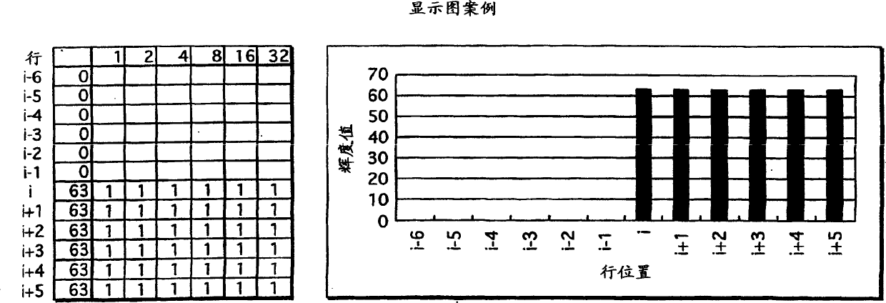
For example, for a pattern displayed with the highest luminance in the current row, that is, the luminance at which all subfields emit light, the occurrence probability of writing errors is high, and Although a writing error has a great impact on vision, no remedial measures can be taken
In addition, for the same pattern, it is impossible to perform optimal correction for the case where the degree of occurrence of writing errors in still images and moving images is different.

Method used


Image

  • Signal processor
  • Signal processor
  • Signal processor

Examples


Embodiment 1

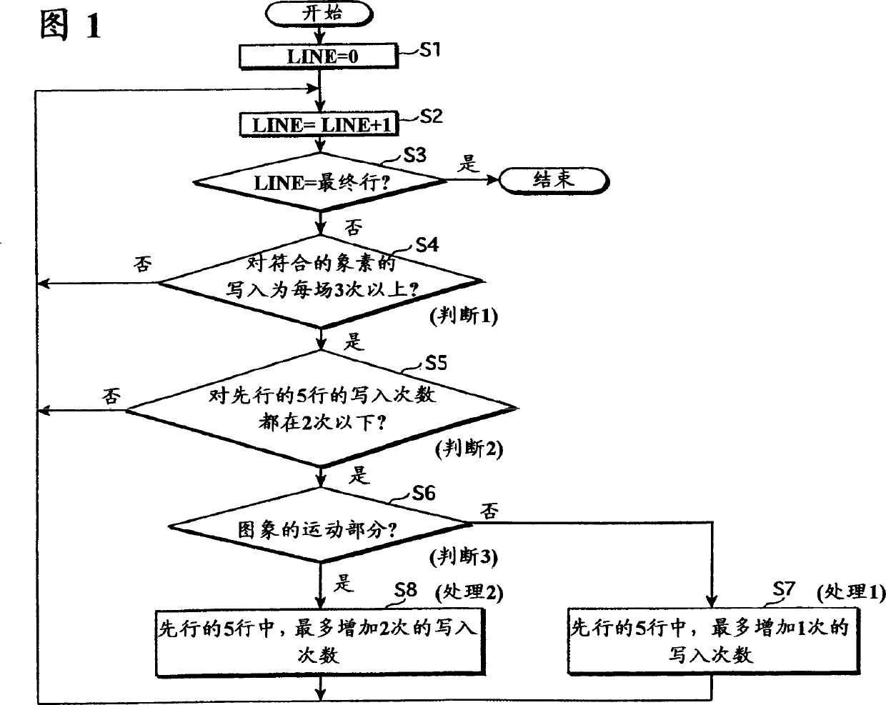
[0054] FIG. 1 is an example of a processing flowchart of a signal processing device employed in an image display device according to a first embodiment of the present invention. The flow of the processing in FIG. 1 will be described below. As the image display device of this embodiment, it is preferable that the front plate and the rear plate are relatively arranged by a partition wall, and the pixels of the same horizontal line on the board are separated by the partition wall, and the pixels of the same column are spatially connected. . In the panel of the plasma display panel device, display information is written to each pixel located on the same horizontal row, and the horizontal row is scanned one by one to realize the related writing operation, and the display information is written to all pixels.

[0055] The display signal is corrected for each line, and the correction process starts from the first scanned line (Line=0, that is, the first line (i=1)) (S1). In additio...

Embodiment 2

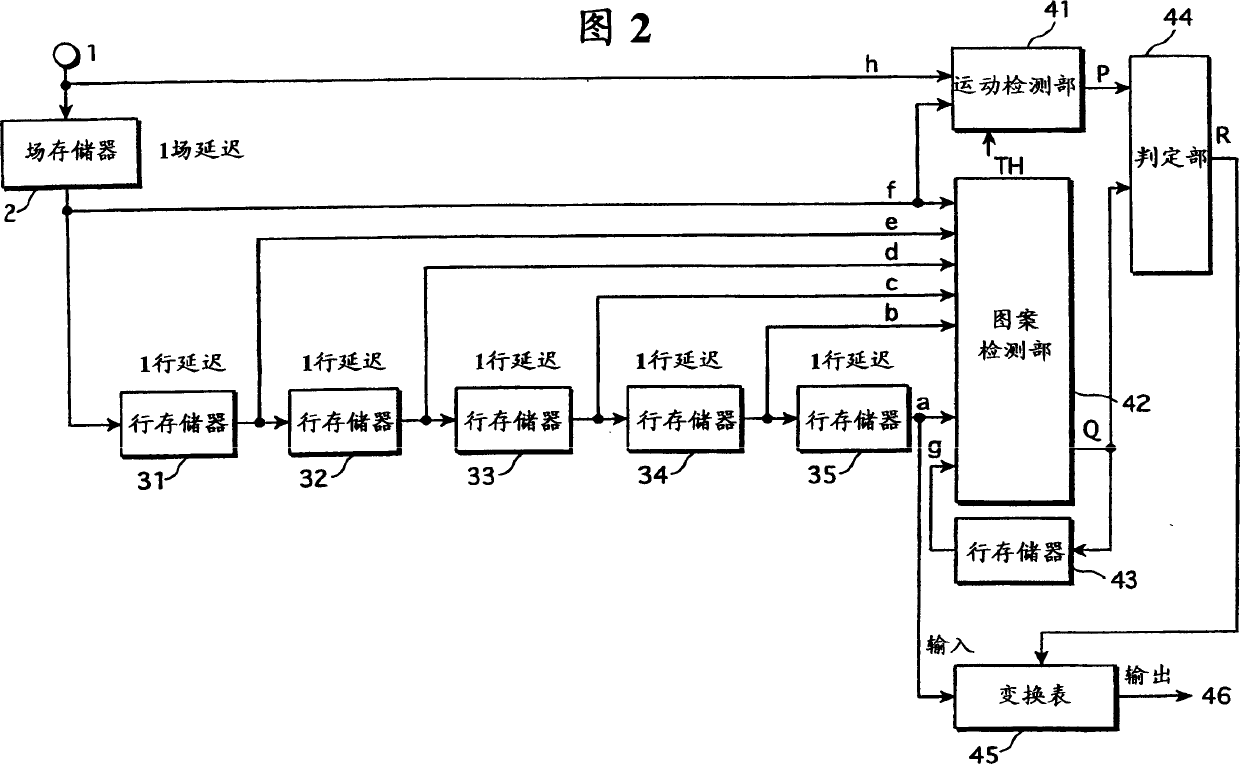
[0075] As a second embodiment, FIG. 13 shows an example in which at least "one line" is executed for the correction line. In such processing, since the correctable range is narrow, the requirements for the display elements are more stringent, but the pattern detection unit 42 and the line memory 31 to 35 that are slave-connected can be simplified, and the signal change accompanying the correction can be limited to a narrow range. within range.

Embodiment 3

[0077] As a third embodiment, FIG. 14 shows an example in which the correction amount changes continuously. That is, as shown in FIG. 14, the input image signal is corrected for 5 lines before i-1 line so that the number of times of writing is 5, 4, 3, 2, or 1.

[0078] Through such processing, the luminance change rate of the edge portion can be suppressed, and at the same time, the rapid change of the write count in the row direction can be suppressed, and the occurrence of write malfunction can be sufficiently suppressed.


PUM


Abstract

In writing scanning using subfields, writing errors may occur due to movement of patterns or images. In patterns prone to writing errors, corrections are made differently for still images and moving images. In particular, for a moving image portion, the writing operation is reliably performed by first performing low-intensity writing in the leading edge portion of the image to activate the pixels.

Description

technical field [0001] The present invention relates to a display device such as a plasma display panel, which writes display information to each pixel located on the same row, realizes the related writing operation through progressive scanning, and writes display information to all pixels, specifically , relates to a signal processing device used in a display device that stably performs a writing operation of display information and performs display. Background technique [0002] When a display device such as a plasma display panel is used for gray scale display, the following method is generally adopted, that is, one field of the image is divided into a plurality of subfields, each subfield has a prescribed luminance weight, and the light emission in each subfield is controlled. The presence or absence of grayscale display (in-field time-sharing grayscale display mode). For example, in order to display 256 gray levels, one field of the input signal is divided into 8 subfi...

Claims


Application Information

Patent Timeline
Patent Type & Authority Applications(China)
IPC IPC(8): G09G3/20
CPCG09G3/20G09G3/2018G09G2320/0261G09G2320/103G09G3/291G09G3/296
Inventor 川原功
Owner PANASONIC CORP
Learn More