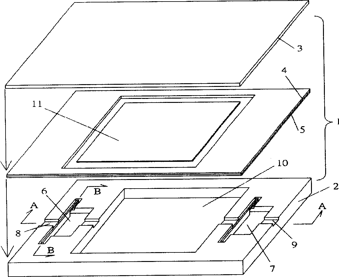
Monolithic unidirectional liquid micropump having suspension T shaped valve film micro valve
A technology of micro-valve and valve membrane, which is applied in the direction of liquid variable capacity machinery, pumps with flexible working elements, pumps, etc.
- Summary
- Abstract
- Description
- Claims
- Application Information
AI Technical Summary
Problems solved by technology
Method used
Image
Examples
Embodiment 1
[0027] Such as Figure 5 As shown, the process of manufacturing the monolithic one-way liquid micropump with suspended T-shaped valve membrane microvalve according to the present invention by adopting the anodic oxidation voltage switching technology with multiple processing areas overlapping each other is as follows:
[0028] 1. The etching and filling of the valve film release silicon groove: select the low-resistance P-type silicon wafer 2 of 0.01-0.015 Ωcm for use; LPCVD deposits silicon nitride 24 with a thickness of 0.2-0.3 microns; silicon groove pattern photolithography, The width of the silicon groove is 0.2-1.2 microns; the deep silicon groove is etched by plasma, partially oxidized at high temperature, and the silicon groove is filled with thermally grown silicon dioxide 24 .
[0029] 2. Silicon recess etching of the valve film: remove the silicon nitride after local oxidation, and perform chemical mechanical polishing on the silicon wafer; LPCVD deposits silicon ni...
Embodiment 2
[0038] Such as Figure 6 As shown, the processing process of the monolithic unidirectional liquid micropump with the suspended T-shaped valve membrane microvalve of the present invention manufactured by monocrystalline silicon thin film transfer technology is as follows:
[0039] 1. Valve membrane groove etching: Choose silicon wafer with (100) or (110) crystal orientation, no limit on resistivity; high temperature and wet oxygen oxidation, silicon dioxide 27 thickness is 0.6 microns; valve membrane groove 28 graphic light Engraving; shallow silicon wet etching, the etching depth is 3-5 microns.
[0040] 2. Silicon pre-etching in the valve cavity area: remove the original silicon dioxide mask; again high-temperature wet oxygen oxidation, silicon dioxide 27 thickness is 1.2 microns; LPCVD deposited silicon nitride 24, 0.2-0.3 microns thick, photo Engraving the micropump cavity, microvalve cavity and microchannel pattern; plasma etching silicon nitride 24, photolithography valv...
PUM
 Abstract
Description
Claims
Application Information
 - R&D Engineer
- R&D Manager
- IP Professional
- Industry Leading Data Capabilities
- Powerful AI technology
- Patent DNA Extraction
Browse by: Latest US Patents, China's latest patents, Technical Efficacy Thesaurus, Application Domain, Technology Topic, Popular Technical Reports.
© 2024 PatSnap. All rights reserved.Legal|Privacy policy|Modern Slavery Act Transparency Statement|Sitemap|About US| Contact US: help@patsnap.com


