
Coupling semiconductor testing device and interface circuit of the semiconductor device to be tested

A technology of interface circuit and test device, which is applied in the field of interface circuit, can solve the problems of inability to test, poor resolution accuracy of output voltage, and inability of tester to test correctly, so as to achieve the effect of reducing test cost

Inactive Publication Date: 2004-06-30
RENESAS TECH CORP
View PDF1 Cites 7 Cited by
  • Summary
  • Abstract
  • Description
  • Claims
  • Application Information

AI Technical Summary

Problems solved by technology

However, if an LSI of a low power supply voltage type is tested with a tester for testing an LSI of a high power supply voltage type, the test cannot be performed due to poor resolution accuracy of the output voltage.
Therefore, a tester with high voltage accuracy is required separately, and the test cost becomes high.
[0006] In addition, LSI is developing toward lower power consumption, and the output current of LSI is suppressed accordingly, and the output impedance of LSI is increased.
Therefore, due to the mismatch between the impedance of the external plug of the tester on the market (mainstream 50Ω) and the output impedance of the LSI (100Ω~300Ω), there is a reflection effect on the output signal waveform of the LSI
Due to this effect, the tester cannot test correctly

Method used


Image

  • Coupling semiconductor testing device and interface circuit of the semiconductor device to be tested
  • Coupling semiconductor testing device and interface circuit of the semiconductor device to be tested
  • Coupling semiconductor testing device and interface circuit of the semiconductor device to be tested

Examples


Embodiment 1

[0027] figure 1 It is a circuit block diagram showing main parts of the semiconductor test system according to the first embodiment of the present invention. figure 1 In this semiconductor test system, a tester 1 and an interface circuit 20 are provided. The tester 1 includes a controller 2, a reference signal generating circuit 3, a test circuit 4, an output buffer 5, a high-speed changeover switch 6, switches 7, 8, a current measuring unit 9, a load circuit (LOAD) 10, and a power supply 11 for the load circuit. , comparators 12, 13, and external plug 14. figure 1 Only one external plug 14 of the tester 1 and its corresponding part are shown in . In practice, a plurality of external plugs 14 are provided.

[0028] The controller 2 outputs various control signals at predetermined timings to control the entire tester 1 . The reference signal generating circuit 3 is controlled by the controller 2, and outputs a reference signal. The test circuit 4 includes a waveform forming...

Embodiment 2

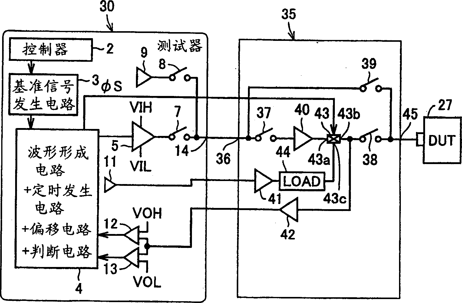
[0045] figure 2 It is a circuit block diagram showing main parts of the semiconductor test system according to the second embodiment of the present invention. figure 2 In this semiconductor test system, a tester 30 and an interface circuit 35 are provided. Tester 30 is from figure 1 The tester removes the high-speed switch 6 and the load circuit 10. The output node of the output buffer 5 is supplied to the external plug 14 via the switch 7 , and the switching signal ΦS generated in the test circuit 4 is directly supplied to the interface circuit 35 . The load circuit power supply 11 and the comparators 12 and 13 are directly connected to the interface circuit 35 . figure 2 Only one external plug 14 of the tester 30 and its corresponding part are shown in . Actually, a plurality of external plugs 14 are provided.

[0046] The interface circuit 35 includes an input terminal 36 , switches 37 to 39 , buffers 40 to 42 , a high-speed changeover switch 43 , a load circuit 44 ,...

change example 1

[0060] Hereinafter, various modification examples will be described. Figure 5 The semiconductor test system has a tester 50 and an interface circuit 51 . Tester 50 is a combination of figure 1 of tester 1 and figure 2 The tester 30, the interface circuit 51 is a combination of the figure 1 The interface circuit 20 and figure 2 The interface circuit 35. This modification 1 can obtain both effects of the first and second embodiments.


PUM


Abstract

The interface circuit includes n buffer circuits, switches for connecting an external pin of a tester to input nodes of n buffer circuits and connecting output nodes of n buffers respectively to n DUTs when a signal is provided from the tester to n DUTs, and successively connecting n DUTs to the external pin of the tester by a prescribed time period when voltage-ampere characteristics of n DUTs are measured. Therefore the number of devices that can be measured by the tester at a time can be increased by n times. As a result, the test cost can be reduced and the test accuracy can be improved.

Description

technical field [0001] The present invention relates to an interface circuit, in particular to an interface circuit coupling a semiconductor testing device and a semiconductor device under test. Background technique [0002] Conventionally, in the field of semiconductor integrated circuit devices (hereinafter referred to as LSIs), the normality of each LSI was tested before shipment, and only normal LSIs were shipped. In this test, a plurality of LSIs are connected to one semiconductor test device (hereinafter referred to as a tester). Usually, one external terminal of the LSI is connected to one external pin of the tester, for example, a signal is supplied from the external pin of the tester to the external terminal of the LSI. [0003] In addition, there is a method of connecting an output plug of a tester in parallel with the LSI in order to reduce the test cost of the LSI (for example, refer to JP-A-2002-189058). [0004] However, simply connecting the output plug of t...

Claims


Application Information

Patent Timeline
Patent Type & Authority Applications(China)
IPC IPC(8): G01R31/28G01R31/319H03K19/0175
CPCG01R31/31924G01R31/31926G01R31/28
Inventor 杉本胜船仓辉彦长泽秀和
Owner RENESAS TECH CORP
Learn More