Phase-width balanced alternating phase shift mask design

A phase shift mask and mask technology, applied in the field of lithography, can solve the problems of different widths, wrong pattern layout, deterioration of process windows, etc., and achieve the effect of avoiding negative effects

Inactive Publication Date: 2004-06-09
INT BUSINESS MASCH CORP
View PDF7 Cites 5 Cited by
  • Summary
  • Abstract
  • Description
  • Claims
  • Application Information

AI Technical Summary

Problems solved by technology

[0047] However, Image 6 The results in reflect the obvious fact that the narrow outer phase line widths of the regions 12A / 12B at both sides of the embedded members VA / VB are very different in width compared to the very wide region 24
Because Image 6 The profile of the light wave intensity from left to right in is not uniform, so this imbalance of phase width at opposite sides of the embedded member VA / VB may cause process window degradation and may introduce pattern placement errors
[0048] Although merging phase domains may be limited, it cannot be completely avoided using techniques that produce phase transitions spanning narrow intervals between 180° phase domains
Thus, in view of the above discussion, it is necessary to provide a method of designing an alternating phase shift mask (altPSM) that minimizes the unbalanced phase width, which is caused by the building blocks, with an acceptable phase width difference. The component has embedded neighbors on only one side and causes process window degradation and image placement errors

Method used


Image

  • Phase-width balanced alternating phase shift mask design
  • Phase-width balanced alternating phase shift mask design
  • Phase-width balanced alternating phase shift mask design

Examples


Embodiment Construction

[0130] In the following description of preferred embodiments of the present invention, a method for optimizing altPSM layout design is provided.

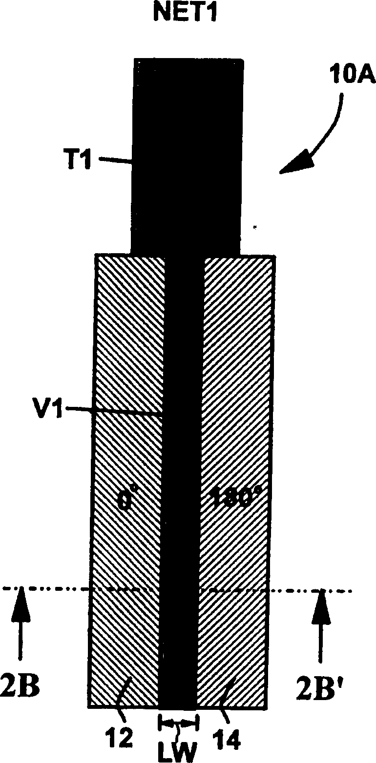
[0131] Figure 7 A method according to the invention is shown for locally rebalancing the phase width by selectively increasing the width of the narrower outer phase region to solve the problem of unbalanced phase width with an acceptable phase width difference, at Image 6 This unbalanced phase width in 2 is caused by features that have embedded neighbors on only one side and lead to process window degradation and image placement errors. Figure 7 A method is shown in which an algorithm according to the present invention is provided such that the 0° phase regions 22A / 22B on the outside of the transistor layout at both sides of the transistors 10A / 10B and Image 6 The 180° phase regions 24 between the two sides of transistors 10A / 10B are matched, thereby overcoming the problem when altPSM masks have significantly uneven phase width...


PUM


Abstract

A method is provided for designing an altPSM mask including a substrate. The method includes the following steps. Provide a circuit layout. Identify critical elements of the circuit layout. Provide a cutoff layout dimension. Identify critical segments of the circuit layout which are critical elements with a sub-cutoff dimension less than the cutoff dimension. Create basic phase shapes associated with the critical segments. Remove layout violations from the phase shapes. Determine whether the widths of phase shapes associated with a critical segment have unequal narrower and wider widths. If YES, then widen each narrower phase shape to match the width of wider phase shape associated with the critical segment and repeat the steps starting with removal of layout violations until the test answer is NO. When the test answer is NO, provide a layout pattern to an output.

Description

technical field [0001] The present invention relates to a lithography method applied in the design and manufacture of very large scale integrated circuits (VLSI), and more particularly to an improved method for forming a phase shift mask (Phase Shifted Mask) design. Background technique [0002] VLSI complementary metal-oxide-semiconductor (CMOS) chips are fabricated on silicon wafers through a series of process steps. These process steps include adding material to the wafer by utilizing addition processes such as low pressure chemical vapor deposition (LPCVD), sputtering operations, and the like. Other steps include removing material from the wafer using processes such as wet etching, reactive ion etching (RIE), and the like. In addition, the wafer can be further processed by material modification methods such as oxidation, ion implantation and similar steps. These physical and chemical operations affect the entire wafer. For example, if the wafer is placed in an acid ba...

Claims


Application Information

Patent Timeline
Patent Type & Authority Applications(China)
IPC IPC(8): G03C5/00G03F1/30G03F9/00G06F9/40G06F17/50
CPCG03F1/30
Inventor 拉斯·W·利布曼卡洛斯·A·方西卡约安纳·格劳尔
Owner INT BUSINESS MASCH CORP
Why Eureka
Try Eureka