
Patsnap Eureka
For R&D, Patsnap Eureka makes reading and utilizing patents & technical documents easy.
Patsnap Eureka AIR
Designed for self-driven R&D workflows. Generate viable solutions, solve complex R&D challenges, empower your innovation with AI.

Patsnap Eureka Materials
Designed for material experts only. Revolutionize your material R&D, from search, analyze, to developing new materials.

TechResearch
Generate reliable direction feasibility study reports for your R&D in just a few steps.

TechSeek
Discover and master advanced knowledge NOW. Basics, ideas, possibilities, all at once.

TechMind
As an expert in R&D Theories, TechMind can generates customized viable solutions instantly.

TechRisk
Analyze your overall solution with one click, know your potential R&D risks in advance.

TechMonitor
Get weekly tech updates, stay abreast of the latest tech innovations and key insights.
Wiring design device and method for integrated circuit
A wiring design, integrated circuit technology, applied in circuits, computer-aided design, computing, etc., can solve the problems of limited wiring freedom, long chip design time, increased memory usage, etc., to reduce memory usage, shorten the Design time, the effect of increasing degrees of freedom
- Summary
- Abstract
- Description
- Claims
- Application Information
AI Technical Summary
Problems solved by technology
Method used
Image


Examples
Embodiment 1
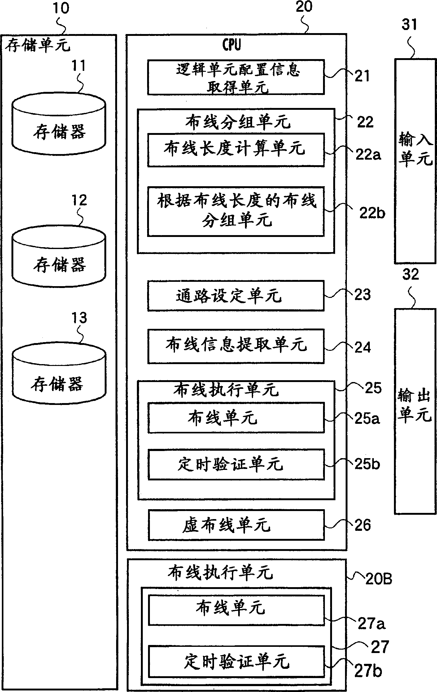
[0026] figure 1 is a configuration diagram of a semiconductor design device according to Embodiment 1 of the present invention.
[0027] LSI design has multiple stages, and the semiconductor design device described here corresponds to a CAD tool for automatic wiring for wiring between logic cells arranged on a chip. In addition, not only wiring but also layout design of logic cells and the like can be performed.
[0028] like figure 1 As shown, the semiconductor design device of the first embodiment has a storage unit 10 having at least a plurality of storage areas 11, 12, 13, etc., and a CPU 20 equivalent to a computer. In addition, as shown in the figure, it is preferable to have a plurality of CPUs because the wiring processing can be processed in parallel. In addition, the input unit 31 and the output unit 32 are provided integrally or as external peripheral devices.
[0029] The storage unit 10 has a plurality of memories 11 to 13, and stores, for example, a program, ...
Embodiment 2
[0058] The wiring design method of the second embodiment is a modified example of the first embodiment. That is, in Embodiment 1, the wiring design method of dividing the wiring between logic cells into the first group and the second group was described by taking 6 wiring layers as an example, but in Embodiment 2, when using 9 wiring layers, the logic Inter-unit wiring is divided into three groups of 1st to 3rd wiring design method.
[0059] In addition, since the structure and design method of the basic design device are the same as those of Embodiment 1, refer to Figure 7 ~ Figure 10 Example 2 will be briefly described.
[0060] First, the logical unit configuration information is obtained (S210), and based on this information, the wiring length of each wiring is calculated, and the wiring whose expected wiring length is less than the reference wiring length is used as the first group, and the wiring that is larger than the reference wiring length and less than twice As t...
Embodiment 3
[0068] The wiring design method of the third embodiment adopts a method different from that of the first and second embodiments for grouping the wiring between logic units.
[0069] In addition, the structure of the basic wiring design device has the same figure 1 The configuration of the wiring design device of the first embodiment shown is substantially the same, but the number of CPUs is the number corresponding to the number of groups.
[0070] Below, refer to Figure 11 The flow chart shown illustrates the wiring design method of Embodiment 3. In addition, the number of wiring layers formed on the semiconductor chip is not limited, but a case of a 6-layer wiring LSI will be described as an example.
[0071] First, logical cell arrangement information such as positions between cell terminals and a wiring connection list between terminals is acquired (S310).
[0072] Next, divide the chip plane into a plurality of areas at the grid-like boundary, divide the wiring betwee...
PUM
 Abstract
Description
Claims
Application Information
 - R&D Engineer
- R&D Manager
- IP Professional
- Industry Leading Data Capabilities
- Powerful AI technology
- Patent DNA Extraction
Browse by: Latest US Patents, China's latest patents, Technical Efficacy Thesaurus, Application Domain, Technology Topic, Popular Technical Reports.
© 2024 PatSnap. All rights reserved.Legal|Privacy policy|Modern Slavery Act Transparency Statement|Sitemap|About US| Contact US: help@patsnap.com