Two-demensional magnetic sensors
A magnetic sensor and sensor element technology, applied in variable inductance/transformer, size/direction of magnetic field, electrical components, etc., can solve the problems of expanding power consumption, large size of MI components, and difficulty in small electronic devices, etc. The effect of reducing power consumption
- Summary
- Abstract
- Description
- Claims
- Application Information
AI Technical Summary
Problems solved by technology
Method used
Image
Examples
Embodiment Construction
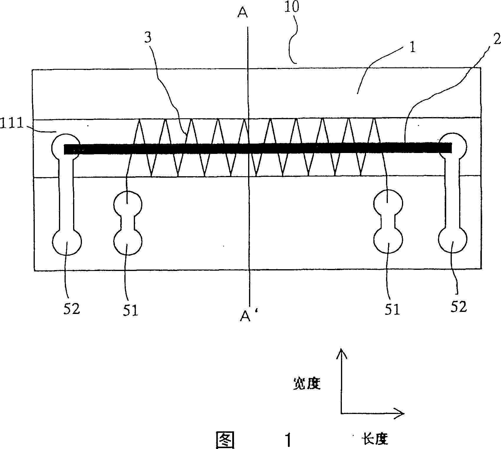
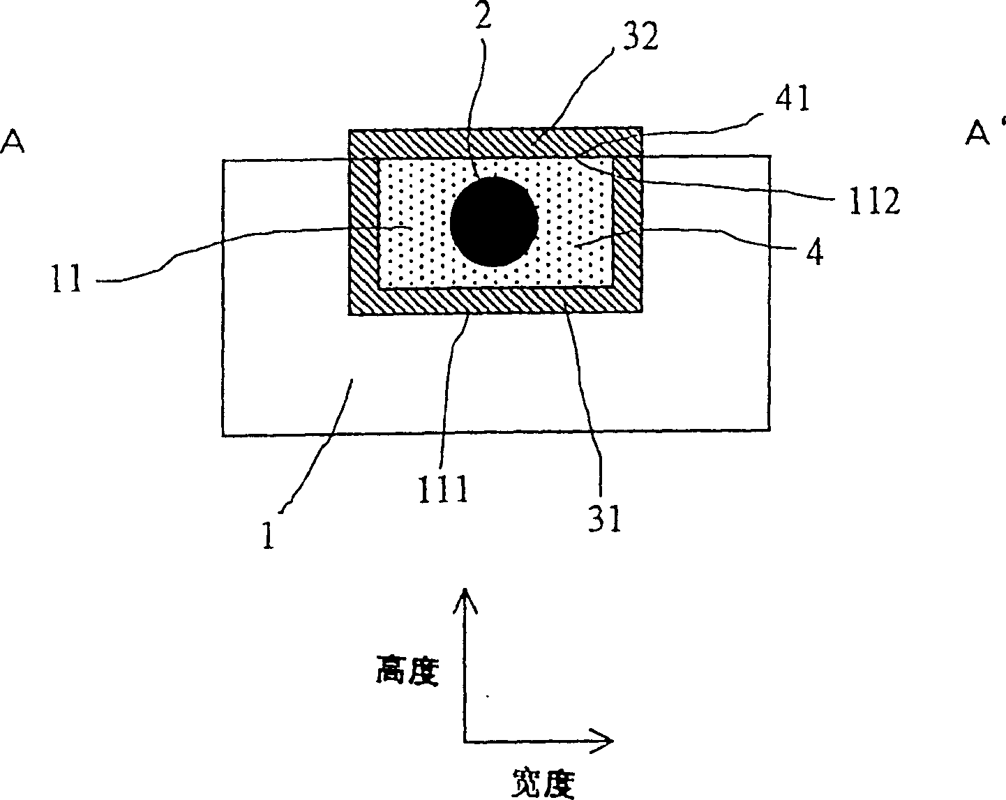
[0021] Hereinafter, the embodiment of the MI element of the present invention is shown in Fig. 1, figure 2 shown.
[0022] The size of the substrate 1 is 0.5 mm in width, 0.5 mm in height and 3 mm in length. As the induction magnet, a CoFeSiB-based alloy and an amorphous alloy magnetic body 2 having a diameter of 30 μm were used. The groove 11 on the substrate has a depth of 50 μm, a width of 70 μm, and a length of 3 mm. The electromagnetic coil 3 is formed by a two-layer structure of one side 31 of the coil formed on the groove surface 111 and the other side coil 32 formed on the groove surface 112 (upper surface 41 of the resin 4), and the average inner diameter (and The area formed by the height and the width is equal to the diameter of a circle) was 66 μm. The winding pitch of the electromagnetic coil 3 with respect to the unit length was 50 μm / coil.
[0023] Between the amorphous alloy magnetic body 2 and the electromagnetic coil 3, an insulating resin 4 is arranged t...
PUM
 Abstract
Description
Claims
Application Information
 - R&D
- Intellectual Property
- Life Sciences
- Materials
- Tech Scout
- Unparalleled Data Quality
- Higher Quality Content
- 60% Fewer Hallucinations
Browse by: Latest US Patents, China's latest patents, Technical Efficacy Thesaurus, Application Domain, Technology Topic, Popular Technical Reports.
© 2025 PatSnap. All rights reserved.Legal|Privacy policy|Modern Slavery Act Transparency Statement|Sitemap|About US| Contact US: help@patsnap.com


