


Quick Research
Generate reliable direction feasibility study reports for your R&D in just a few steps.

Technical Q&A
Discover and master advanced knowledge NOW. Basics, ideas, possibilities, all at once.

Find Solutions
As an expert in R&D theories, this can generate solutions to your technical problems instantly.

Evaluate Feasibility
Analyze your overall solution with one click, know your potential R&D risks in advance.

Monitor Landscape
Get weekly tech updates, stay abreast of the latest tech innovations and key insights.
Circuit-board having internal electronic element and making method thereof
A technology of electronic components and circuit boards, which is applied in the field of circuit boards installed with internal electronic components and its manufacturing field, can solve the problems of damage to heat dissipation efficiency, difficulty, and difficulty in complete coverage, and achieve the effect of improving connection reliability
- Summary
- Abstract
- Description
- Claims
- Application Information
AI Technical Summary
Problems solved by technology
Method used
Image

Examples
example 1
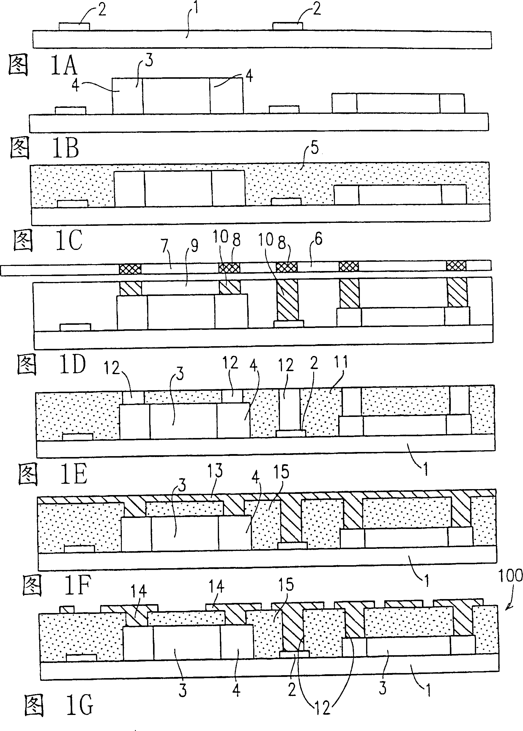
[0066] 1A to 1G are cross-sectional views illustrating process steps of a manufacturing method of a circuit board 100 mounted with built-in electronic components (hereinafter referred to as "circuit board 100 mounted with built-in electronic components") according to a first embodiment of the present invention. FIG. 1G shows the completed state of the circuit board 100 mounted with built-in electronic components.
[0067] As shown in Figure 1G, the circuit board 100 that is installed with built-in electronic components includes: flat core (support plate) 1, the wiring pattern 3 that is arranged on the flat core 1, and various electronic components 3 that are arranged on the flat core 1 . In this embodiment, two electronic components with different heights are arranged on the flat core 1 . The electronic components 3 are arranged on the surface of the flat core 1, but not in the wiring figure 2 within the area.
[0068] The circuit board 100 mounted with built-in electronic...
example 2
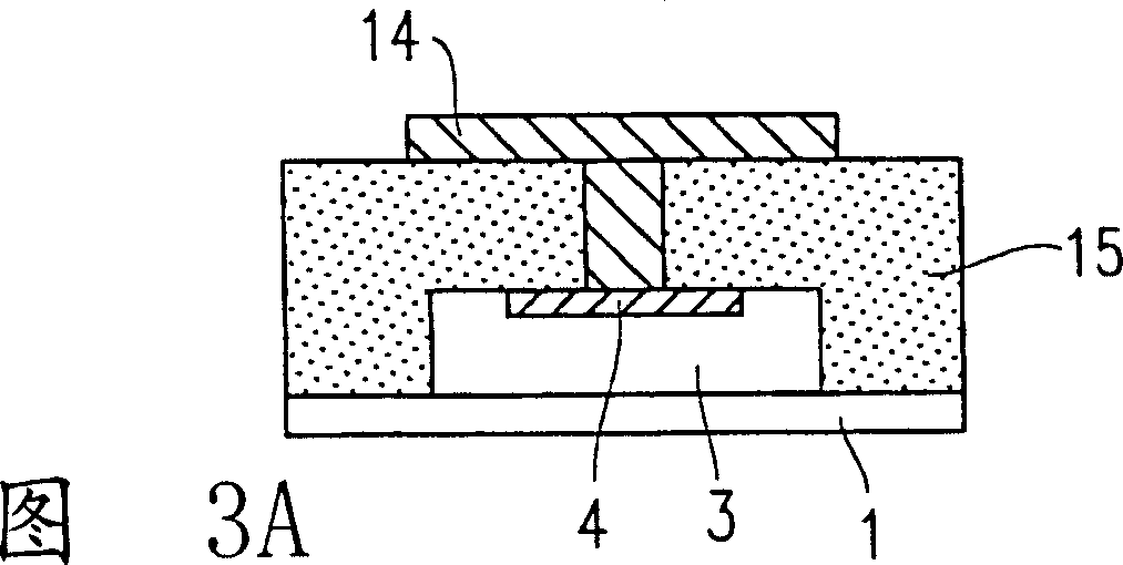
[0086] Figure 4 is a sectional view illustrating the structure of a circuit board mounted with built-in electronic components according to a second embodiment of the present invention. In the first embodiment, the insulating layer 15 is provided on the entire surface of the flat core 1 . In the second embodiment, the insulating layer 15 is provided only on the electronic component 3 and the necessary area of the flat core 1, and the insulating layer 30 made of a resin plate is provided in the remaining area of the flat core 1.
[0087] Due to such a structure, the production cost of the circuit board on which the built-in electronic components are mounted can be reduced. and increase its rigidity. When the circuit board mounted with built-in electronic components is punched along the line of the isolation layer 30, the desired shape can be obtained without cracks.
example 3
[0089] Figure 5 is a sectional view illustrating the structure of a circuit board mounted with built-in electronic components according to a third embodiment of the present invention. In the first embodiment, both sides of the electronic component 3 have connection lead-out terminals. In the third embodiment, an electronic component 3 has a plurality of connection terminals 4 on one surface, and can be formed into substantially the same shape as a BGA package without punching.
[0090] Electronic components 3 having such a shape are provided on the flat core 1 . Like the first embodiment, through the openings 12 formed in the insulating layer 15, the connection terminals 4 and the wiring patterns 14 are respectively connected to each other. In the third embodiment, there are a plurality of connection portions between the connection terminal 4 and the wiring pattern 14 .
[0091] In this embodiment, the diameter of each connection portion from the connection terminal 4 to t...
PUM
 Abstract
Description
Claims
Application Information
 - R&D Engineer
- R&D Manager
- IP Professional
- Industry Leading Data Capabilities
- Powerful AI technology
- Patent DNA Extraction
Browse by: Latest US Patents, China's latest patents, Technical Efficacy Thesaurus, Application Domain, Technology Topic, Popular Technical Reports.
© 2024 PatSnap. All rights reserved.Legal|Privacy policy|Modern Slavery Act Transparency Statement|Sitemap|About US| Contact US: help@patsnap.com