
Integrated wiring method of standard units with carrying optimization of time delay based on considering coupling effect

A technology of coupling effect and standard unit, which is applied in special data processing applications, instruments, electrical digital data processing, etc., can solve the problems of application limitations, no consideration of the influence of coupling effect delay, etc., and achieve circuit delay optimization and total delay Reduce, reduce the effect of coupling capacitance

Inactive Publication Date: 2003-05-07
TSINGHUA UNIV
View PDF0 Cites 19 Cited by
  • Summary
  • Abstract
  • Description
  • Claims
  • Application Information

AI Technical Summary

Problems solved by technology

However, due to the lack of consideration of the coupling effect on the delay, the application of this method is limited under new process conditions.

Method used

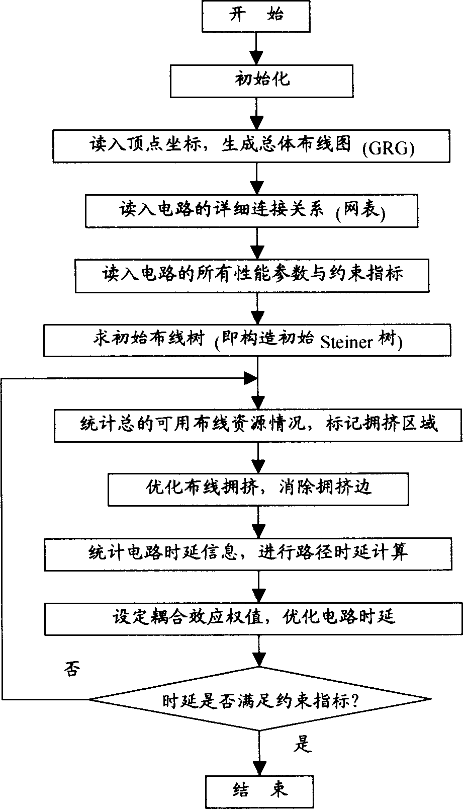

Image

  • Integrated wiring method of standard units with carrying optimization of time delay based on considering coupling effect
  • Integrated wiring method of standard units with carrying optimization of time delay based on considering coupling effect
  • Integrated wiring method of standard units with carrying optimization of time delay based on considering coupling effect

Examples


Embodiment Construction

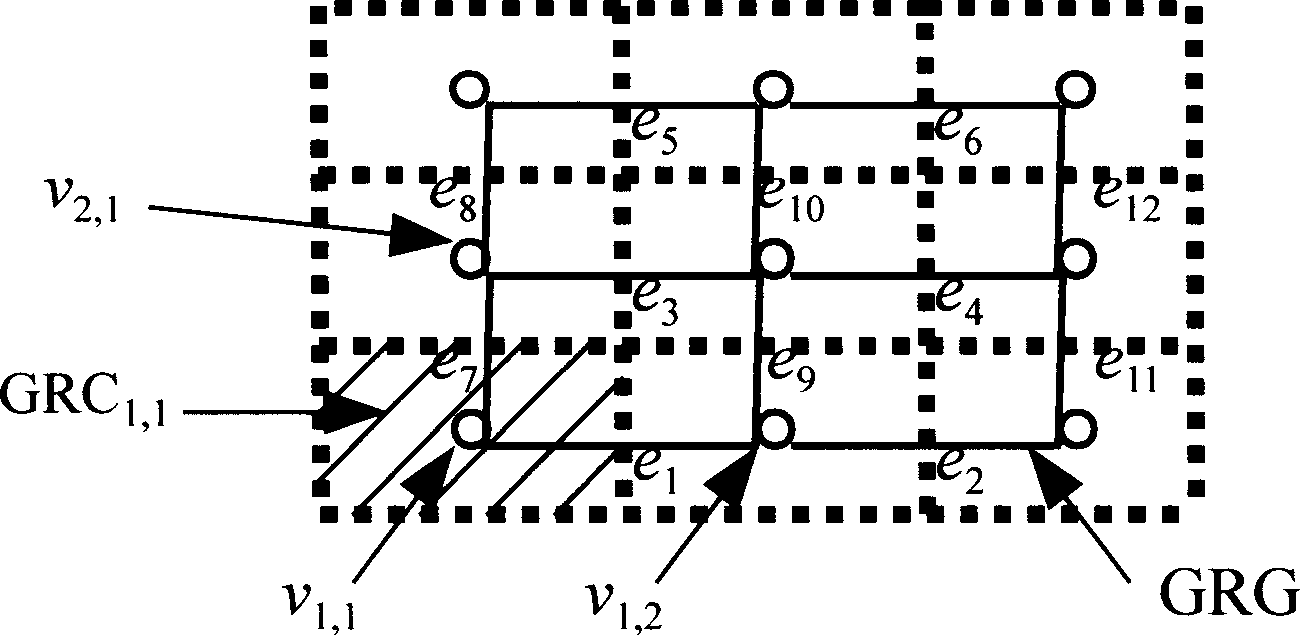
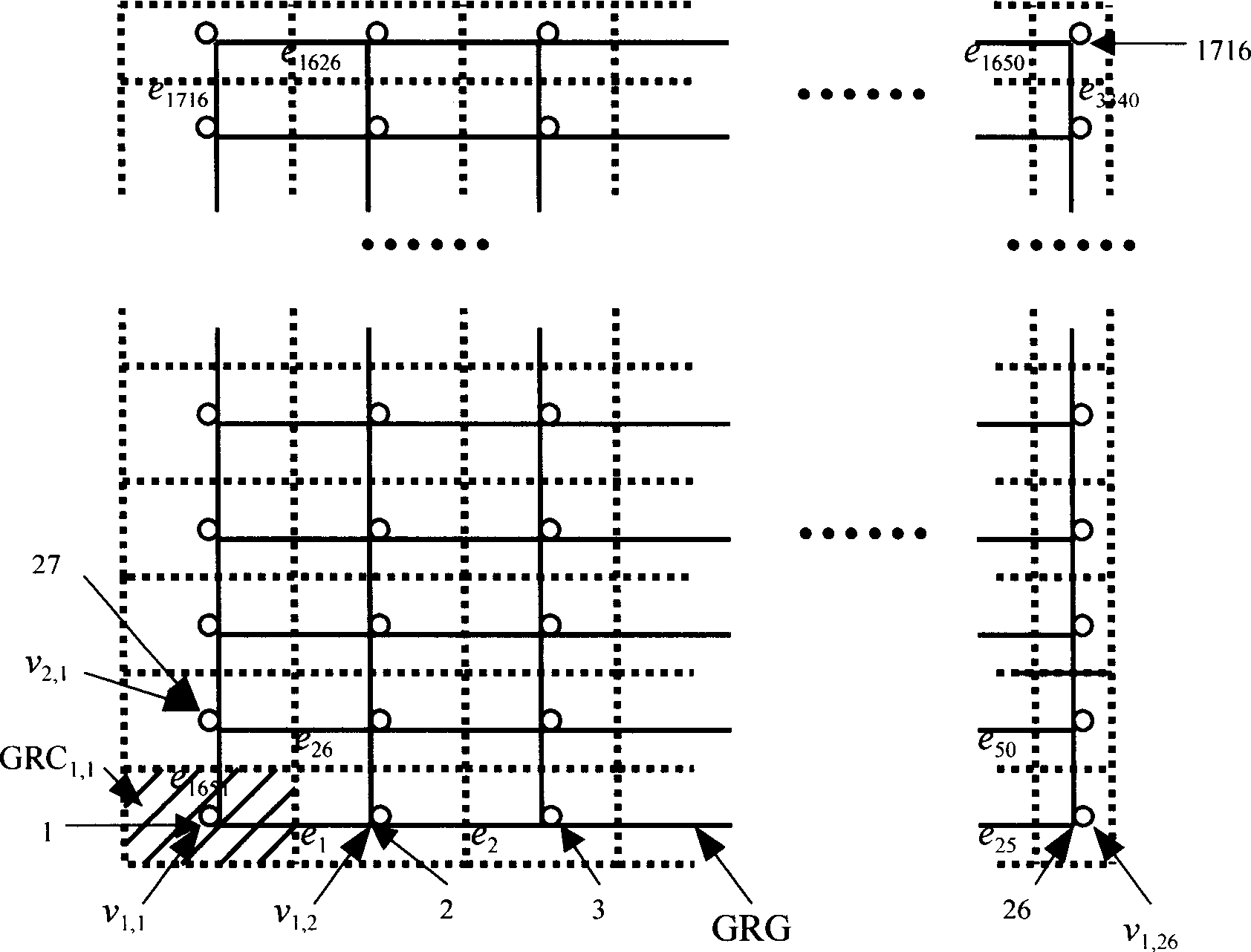
[0052] For the current multi-layer wiring technology in IC design, the routing area is no longer a wiring channel between units, but a complete chip plane. The grid method can be used to divide the entire chip plane into several regions called the overall wiring unit GRC according to rows and columns, and then generate the dual graph of the GRC, that is, as figure 1 Shown in the general wiring diagram GRG. GRG by N nr ×N nc nodes and the edges connecting these nodes. with GRC nr,nc The corresponding node v nr,nc The coordinates are GRC nr,nc the center point of . Connect the two nodes V nr1,nc1 and v nr2,vnc2 The edge of is called e k ; l k represents two nodes v nr1,nc1 and v nr2,nc2 The distance between, called e k length; C k represents two nodes v nr1,nc1 and v nr2,nc2 The number of connections of the line network that can pass through the adjacent sides of the corresponding two GRCs is called e k capacity. Therefore, the pin point Pin to be connected in...


PUM


Abstract

Standard unit general routing method of coupling effect in time delay optimization characterizes in making up time delay optimization routing tree under the condition that any of the wire nets is not restrained to further optimize outing congestion to estimated the link electricity parameter with successively connected linking load model based on empiric analog after elimianting congestion edge, to compute the link delay with congruence variation technology to compute gate delay etc. three steps to calculate the path general delay value with looking-up table+interpolation based on the delay information table given by user, then enhancing to considerate the key path up wire net weighted value of the couple effect to reduce routing density adjacent to the wire net, so as to reduce couple condenser and general path delay to optimize the circuit time delay.

Description

technical field [0001] In the field of integrated circuit computer aided design (IC CAD), especially in the field of standard cell (SC) overall layout. Background technique [0002] In integrated circuit (IC) design, physical design It is the main link in the IC design process, and it is also the most time-consuming step. Computer-aided design techniques related to physical design are called layout design . In layout design, general wiring is an extremely important link, and its results are crucial to the final Detailed wiring The success or failure of the chip and the performance of the chip have a great impact. [0003] The manufacturing process of integrated circuits is currently moving from Very Deep Submicron (VDSM) Enter nanometer stage; the design scale of integrated circuits is also being determined by Very Large Scale (VLSI) , Very Large Scale (ULSI) Towards G Scale (GSI) direction development. Under such conditions, on the one hand, in integrat...

Claims


Application Information

Patent Timeline
IPC IPC(8): G06F17/50
Inventor 洪先龙经彤许静宇张凌胡昱
Owner TSINGHUA UNIV
Learn More