Illuminating device
A technology of light-emitting devices and light-emitting elements, which is applied in the direction of electric solid-state devices, semiconductor devices, electroluminescent light sources, etc., and can solve the problems of short life and insufficient life.
- Summary
- Abstract
- Description
- Claims
- Application Information
AI Technical Summary
Problems solved by technology
Method used
Image
Examples
Embodiment 1
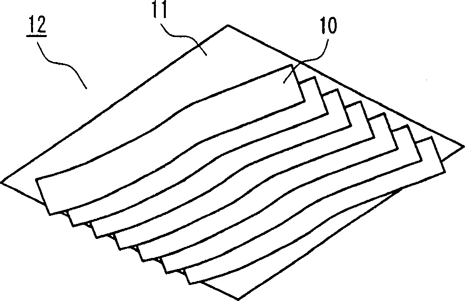
[0054] On a polycarbonate substrate with a length of 1m, a width of 1m, and a thickness of 0.3mm, ITO is formed as a transparent anode, and poly(P-styrene) with a thickness of 80nm is coated as a light-emitting layer, and 10nm is evaporated as an electron injection cathode. Thickness of Ca, followed by evaporation of 100nm thickness of Al as a cathode, to make a light-emitting film. This luminescent film was cut into strips of 5 cm in length and 30 cm in width to form strip-shaped light-emitting elements. Secondly, if figure 1 As shown, the strip-shaped light-emitting element 10 is inserted longitudinally into a groove-shaped jig of acrylic resin substrate 11 having a metal reflective surface of 30 cm in length and 25 cm in width, and the light-emitting device 12 of the present invention is produced. At this time, the light-emitting surface of the strip-shaped light-emitting element is arranged so as to be located in a vertical direction with respect to the above-mentioned ba...
Embodiment 2
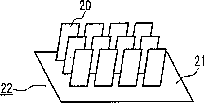
[0059] On a glass substrate with a length of 30 cm, a width of 40 cm, and a thickness of 0.5 mm, after forming an ITO film as an anode, a N, N'-2(4'-diphenylamine-4-2-phenyl)-N,N A 50nm-thick hole transport layer composed of '-2phenylbenzidine, followed by 4,4'-2(carbazole-9-isoyl)-2benzene and 3(2-phenylpyridine)iridium as the light-emitting layer (2Benzene-4-aurate)2(2-methyl-8-hydroxyquinoline)aluminum was evaporated to a thickness of 10 nm as a blocking layer at a mass ratio of 95:5 to a thickness of 30 nm. Next, a laminated cathode composed of Li with a thickness of 1 nm and Al with a thickness of 100 nm was formed to produce a rectangular light-emitting element. This luminescent plate was cut into a rectangular shape of 0.8 cm in length and 1.2 cm in width to obtain a rectangular luminescent plate. Secondly, if figure 2 As shown, the minor axis direction of the rectangular light-emitting element 20 is inserted into a groove-shaped jig of a base material 21 made of acr...
Embodiment 4
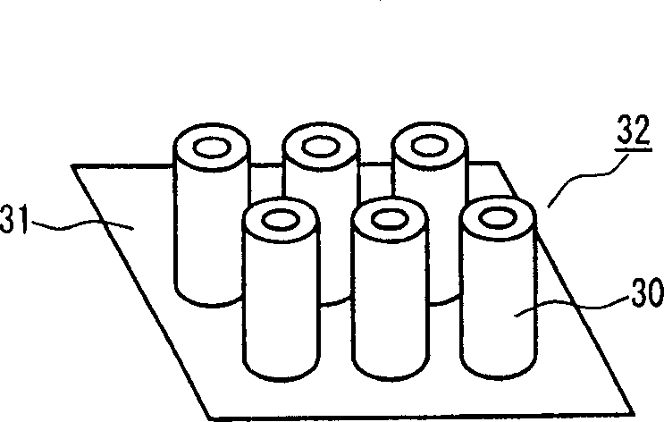
[0069] Polycarbonate is molded into a porous substrate with holes of 1 mm intervals, 2 mm in radius and 1.5 cm in depth. Al was evaporated to a thickness of 200 nm on the surface of the porous substrate having pores, and then Li was evaporated to a thickness of 1 nm as a cathode. Next, 3(8-quinoline)aluminum was evaporated to a thickness of 40 nm as an electron transport layer, and (2phenyl-4-aurate)2(2-methyl-quinoline)aluminum to a thickness of 10 nm was evaporated as a blocking layer. As a light-emitting layer, 4,4'-2(carbazole-9-acyl)-2benzene and 3(2-phenylpyridine)iridium were evaporated to a thickness of 30nm in a mass ratio of 95:5 to form a layer composed of N,N'- A hole transport layer with a thickness of 50 nm composed of 2(4'-2phenylamino-4-2phenyl)-N,N'-2phenylbenzidine. Next, ITO is formed as a transparent anode, and SiN is formed as a protective film with a thickness of 1 μm. Finally, the pores of the porous substrate are filled with cycloolefin polymer to prod...
PUM
| Property | Measurement | Unit |
|---|---|---|
| thickness | aaaaa | aaaaa |
Abstract
Description
Claims
Application Information
 - R&D Engineer
- R&D Manager
- IP Professional
- Industry Leading Data Capabilities
- Powerful AI technology
- Patent DNA Extraction
Browse by: Latest US Patents, China's latest patents, Technical Efficacy Thesaurus, Application Domain, Technology Topic, Popular Technical Reports.
© 2024 PatSnap. All rights reserved.Legal|Privacy policy|Modern Slavery Act Transparency Statement|Sitemap|About US| Contact US: help@patsnap.com


