Quantum-size electronic devices and operating conditions thereof

An electronic device and device technology, applied in the field of integrated circuit multifunctional electronic components

Inactive Publication Date: 2002-02-27
QUATRAN HK LTD
View PDF0 Cites 12 Cited by
  • Summary
  • Abstract
  • Description
  • Claims
  • Application Information

AI Technical Summary

Problems solved by technology

This model is quite accurate ...

Method used


Image

  • Quantum-size electronic devices and operating conditions thereof
  • Quantum-size electronic devices and operating conditions thereof
  • Quantum-size electronic devices and operating conditions thereof

Examples


Embodiment Construction

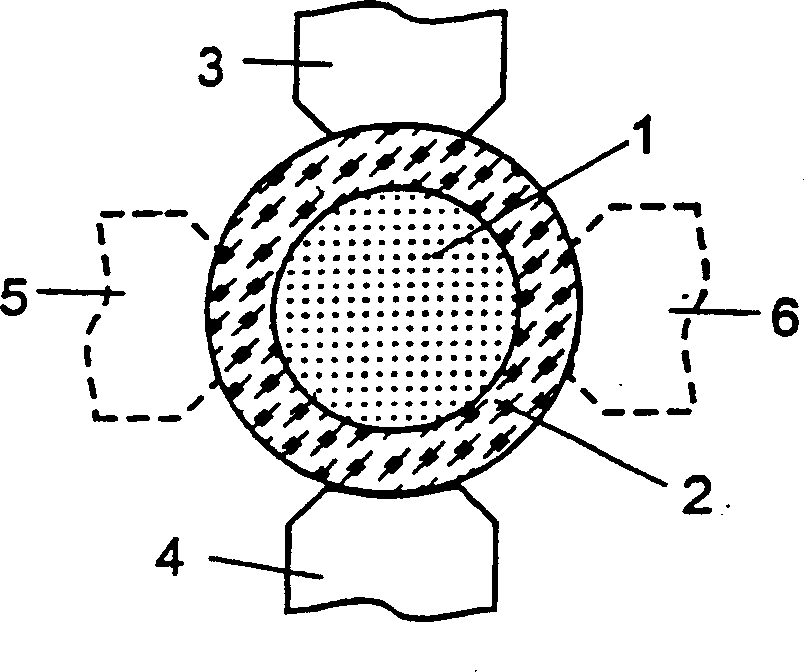
[0059] According to an embodiment of the present invention, a quantum-scale electronic device comprises electrodes, at least one particle cluster and a tunnel transparent layer, characterized in that the particle cluster has at least one unique scale determined according to the following formula:

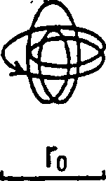
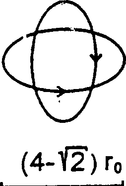
[0060] r=a.r o where r o is the electron wave (ring) radius, its expression is: in is Planck's constant, m e is the mass of the electron, α is the fine structure constant = 1 / 137036, C is the speed of light, and a is the coefficient, and its specified range is:

[0061] 1≤a≤4.

[0062] Accordingly, the thickness of the tunnel transparent layer is at r o Below, the distance between the electrodes is also r o the following.

[0063] According to the present invention, particle clusters can be made of metals, semiconductors, superconductors, and polymeric organic materials. Furthermore, the cluster can be made as an inner cavity with an outer shell in the form of a ...


PUM

PropertyMeasurementUnit
Resistivityaaaaaaaaaa

Abstract

Quantum-size electronic devices comprise electrodes and at least one cluster separated from the said electrodes by a tunnelly transparent gap. The characteristic dimensions for elements of quantum-size devices are determined by the formula in the range 1x4 r0, wherein r0 = h/(me alpha <2>c), wherein h is the Planck's constant, me is the electron mass, alpha = 1/137,036 is the fine structure constant, c is the light speed. The cluster may be made of a semiconductor material, conductor, superconductor, high-molecular substance or a sheath with a tunnelly transparent dielectric. The matured theory provides possibilities for designing logical devices operating in the mode of transfer and/or storing of several electrons at normal conditions and high temperatures. The operating regimes of the devices are determined. The invention provides basic condition for constructing of high-temperature superconducting elements and devices based thereon.

Description

technical field [0001] The present invention relates to the field of electronic components and conductors, and in particular to integrated circuit (IC) multifunctional electronic components with the smallest accessible outline size, highest speed and highest operating temperature. Two-dimensional (planar) and three-dimensional electronic devices and ICs are constructed with components and conductors that work based on quantum-scale resonance effects. The IC is designed to process and convert analog and digital information and to transmit electrical signals and energy without loss. Background technique [0002] IC components tend to be reduced in size. However, when the scale of IC components is reduced to less than 100nm, the charge carriers begin to appear discrete and their quantum mechanical properties affect the structural properties of active devices (ie, transistors). [0003] At the same time, when the size is less than 100nm, the individual transistor components ar...

Claims


Application Information

Patent Timeline
IPC IPC(8): H01L29/76H01L39/22H01L45/00H01L51/00
CPCB82Y10/00H01L39/221H01L51/0595H01L29/7613H01L49/006H01L45/00H10N60/11H10N70/00H10N99/05H10K10/701H01L29/15
Inventor 亚历山大·米哈伊洛维奇·伊尔雅诺克
Owner QUATRAN HK LTD
Why Eureka
Try Eureka