
Photoresist supply system and method

A supply system, photoresist technology, applied in electrical components, semiconductor/solid-state device manufacturing, circuits, etc., can solve problems such as pattern distortion, inability to provide etching masks, etc., to avoid excessive mixing and agitation.

Inactive Publication Date: 2006-11-22
MACRONIX INT CO LTD
View PDF0 Cites 0 Cited by
  • Summary
  • Abstract
  • Description
  • Claims
  • Application Information

AI Technical Summary

Problems solved by technology

These pre-existing microbubbles can cause defects in the fabricated structure in many ways, including: distorting the pattern (this pattern is defined by avoiding sharp corners at the edge of the pattern, to be transferred or fabricated on a wafer or disk surface pattern), inability to provide the desired etch mask, improper photoresist removal caused by avoiding photoresist sticking to the wafer or disk surface during development, and other defects

Method used


Image

  • Photoresist supply system and method
  • Photoresist supply system and method
  • Photoresist supply system and method

Examples


Embodiment Construction

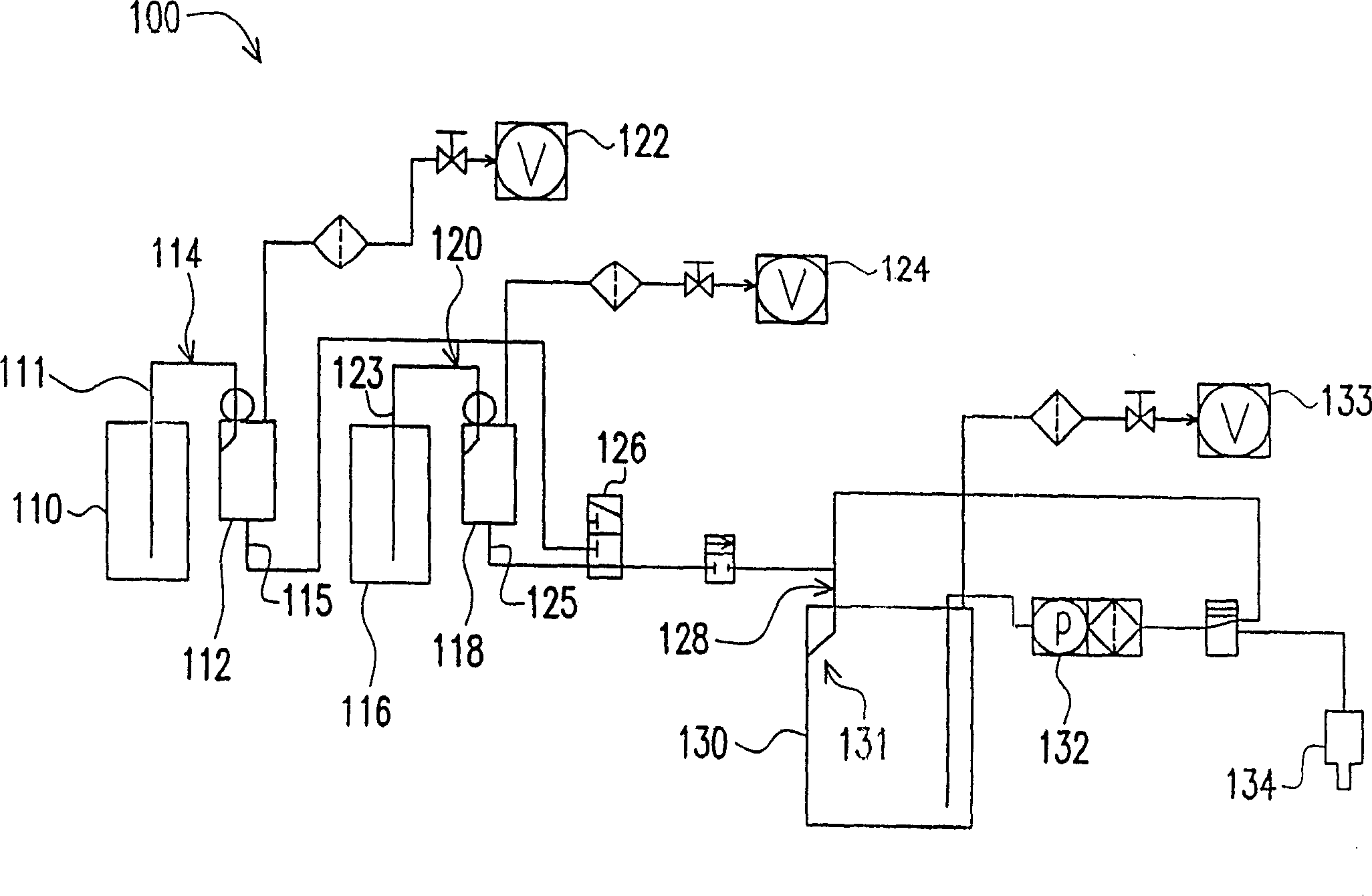
[0042] Several preferred embodiments of the photoresist supply system of the present invention will be described as follows. In a preferred embodiment, a supply system includes a negative pressure supply system and a photoresist reservoir with inlet design features to avoid microbubbles from the photoresist supply system. In order that the present invention may be fully understood, specific details are further described below. However, it must be understood that one skilled in the art can practice the invention without some or all of these specific details. In other instances, well-known technologies have not been described in detail so as not to unnecessarily obscure the present invention.

[0043] figure 1 Shown is a schematic diagram of a photoresist supply system according to a preferred embodiment of the present invention. Such as figure 1 As shown, a first storage bottle 110 is supplied to a first reservoir 112 via a first inlet conduit 114 . The second storage bottle...


PUM


Abstract

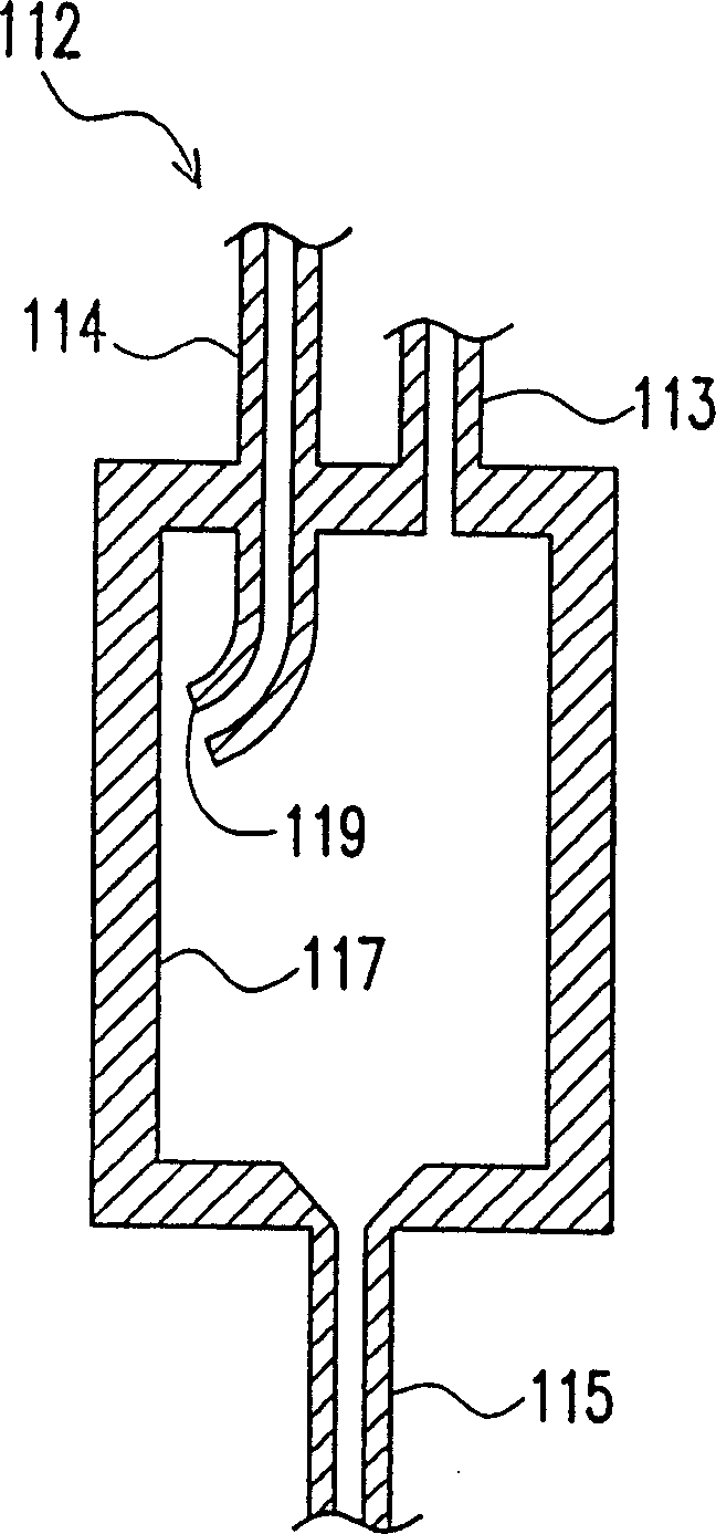
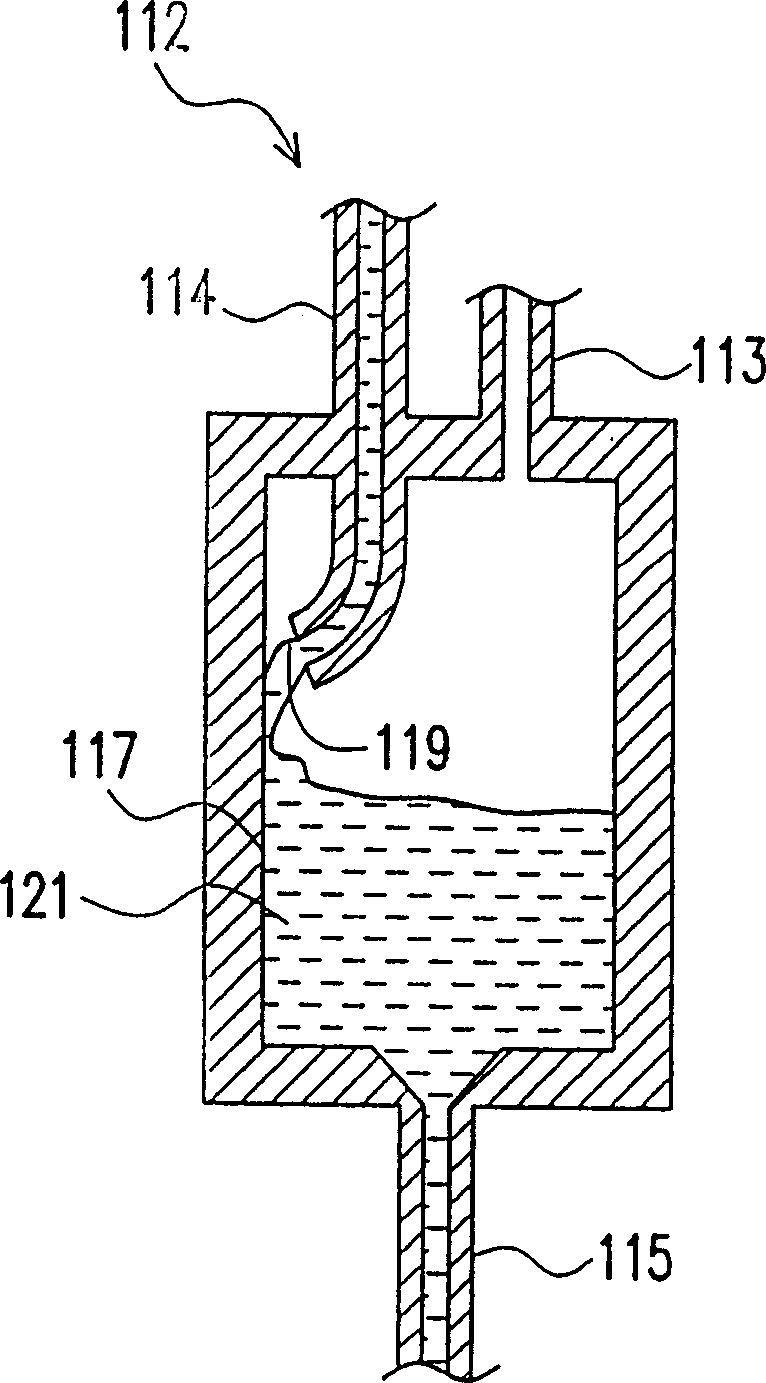
A photoresist supply system includes a storage bottle and a reservoir, and the storage bottle is connected to the reservoir. A vacuum pump is connected to the reservoir to generate a vacuum state in the reservoir for sucking the photoresist out of the storage bottle and into the reservoir. An inlet into the reservoir causes photoresist to flow along an inner wall of the reservoir. The photoresist flows out of the reservoir into a dispensing reservoir, and the photoresist is pumped to a dispensing nozzle for application to a wafer or substrate.

Description

technical field [0001] The present invention relates to the manufacture of semiconductor wafers and optical disks, and more particularly to a supply system and method for photoresist or other similar operating fluids. Background technique [0002] In the fabrication process of semiconductor wafers, photoresists are used to form patterns on the surface of semiconductor wafers. The lithography process usually determines the surface size of circuit manufacturing and circuit structures, and is a key process for wafer manufacturing. As integrated circuits become smaller and the integration of transistors in integrated circuits increases, the precision of lithography and the ability to pattern smaller features becomes more important for advanced semiconductor fabrication processes. [0003] Generally speaking, the lithography process includes coating a photoresist layer on the surface layer of a semiconductor wafer, and then exposing the photoresist through a pattern to transfer ...

Claims


Application Information

Patent Timeline
Patent Type & Authority Patents(China)
IPC IPC(8): H01L21/027G03F7/16
Inventor 刘顺财
Owner MACRONIX INT CO LTD
Learn More