LC passive low pass flter on chip and prepn. thereof

A low-pass filter and low-pass filter circuit technology, which is applied to waveguide-type devices, circuits, electrical components, etc., can solve the problem of large insertion loss of the filter substrate, and achieve the elimination of insertion loss, small size, and production cost. low effect

Inactive Publication Date: 2006-09-06
EAST CHINA NORMAL UNIV
View PDF0 Cites 0 Cited by
  • Summary
  • Abstract
  • Description
  • Claims
  • Application Information

AI Technical Summary

Problems solved by technology

However, the insertion loss of the substrate of the filter is relatively large

Method used


Image

  • LC passive low pass flter on chip and prepn. thereof
  • LC passive low pass flter on chip and prepn. thereof

Examples


Embodiment

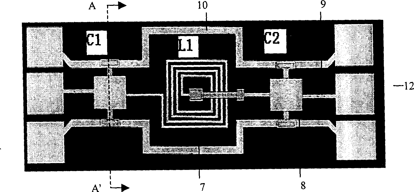
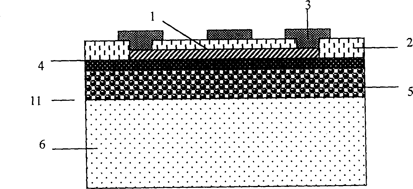
[0024] Example An on-chip LC passive low-pass filter based on oxidized porous silicon / porous silicon with the above structure prepared by the above method.

[0025] Composite substrate 11 is fabricated first. The low-resistance silicon wafer 6 is a silicon wafer with a crystal orientation of 100 and a slow resistivity ρ of 0.01Ω·cm. Immerse the low-resistance silicon wafer 6 in 40% HF ethanol solution, HF:C 2 h 5 The volume ratio of OH = 1:1, the current density of the anodic oxidation current is 25mA cm -2 . The anodizing time, that is, the etching time is 20 minutes, and a porous silicon layer 5 with a thickness of 20 μm is formed on the low-resistance silicon wafer 6 . Use the low resistance silicon chip 6 with H 2 o 2 After soaking and rinsing with deionized water, put it into an oven for drying at 200°C. Then, the porous silicon layer 5 was oxidized with wet oxygen at 1180 for 30 minutes, and an oxidized porous silicon film 4 with a thickness of 1 μm was formed on ...


PUM

PropertyMeasurementUnit
electrical resistivityaaaaaaaaaa
thicknessaaaaaaaaaa
thicknessaaaaaaaaaa

Abstract

The filter includes micro inductance on chip, MIM capacitance on chip, coplane waveguide transmission line on chip, and composite substrate, which is composed of oxidation porous silicon film, porous silicon layer and silicon chip in low resistance. Porous silicon layer is in between oxidation porous silicon film and silicon chip in low resistance. On chip LC passive lowpass filtering circuit composed of micro inductance on chip, MIM capacitance on chip, coplane waveguide transmission line on chip is fabricated on the oxidation porous silicon film through technique compatible to CMOS technique. Advantages of the method are: easy of manufacture, small size, and small insertion loss.

Description

technical field [0001] The present invention relates to an on-chip LC passive low-pass filter and its preparation method, to be precise, an on-chip LC passive low-pass filter based on oxidized porous silicon / porous silicon and its preparation method, which belongs to the on-chip passive low-pass filter in radio frequency communication Technical fields of source devices and their fabrication Background technique [0002] In radio frequency and microwave communication, the on-chip LC passive low-pass filter can be composed of on-chip inductors and on-chip MIM capacitors, that is, on-chip LC circuits and substrates. The key to the circuit (MMIC / RFIC). [0003] The on-chip LC passive low-pass filter realized by using on-chip inductor and on-chip MIM capacitor technology has the characteristics of simple manufacturing process and low cost, and more importantly, it is compatible with today's CMOS technology. In recent years, with the development of mobile co...

Claims


Application Information

Patent Timeline
Patent Type & Authority Patents(China)
IPC IPC(8): H01P1/20H01P11/00
Inventor 石艳玲刘赟王勇丁艳芳
Owner EAST CHINA NORMAL UNIV
Why Eureka
Try Eureka