LED in III group nitride and its manufacturing method

A technology of light-emitting diodes and manufacturing methods, which is applied in the direction of electrical components, circuits, semiconductor devices, etc., can solve the problems of affecting the light-emitting characteristics of components, reducing the effective carrier concentration of p-type nitrides, and low doping concentration, so as to improve current dispersion ability, reduction of hydrogen passivation, production and quality improvement

Inactive Publication Date: 2005-06-29
EPISKY
View PDF0 Cites 0 Cited by
  • Summary
  • Abstract
  • Description
  • Claims
  • Application Information

AI Technical Summary

Problems solved by technology

In addition, in the uppermost layer structure of the existing group III nitride light-emitting diodes, most of them are p-type nitrides, such as the p-type ohmic contact layer 22. Since the doping concentration of p-type nitrides is often lower than that of n-type nitrides, it cannot Provides effective current spreading
In addition, in the structure of the existing III-nitride light-emitting diode, since the p-type nitride is exposed to the outside world, the external hydrogen ions are often drilled into the p-type nitride during the cleaning or etching steps. The effective carrier concentration of p-type nitride is reduced, which affects the luminous characteristics of the device
Since the above shortcomings will lead to poor luminous efficiency of III-nitride light-emitting diodes, how to effectively further improve the luminous efficiency of III-nitride light-emitting diodes is still the goal that everyone expects.

Method used


Image

  • LED in III group nitride and its manufacturing method
  • LED in III group nitride and its manufacturing method
  • LED in III group nitride and its manufacturing method

Examples


Embodiment Construction

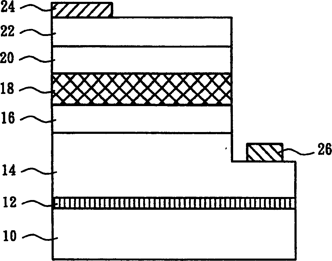
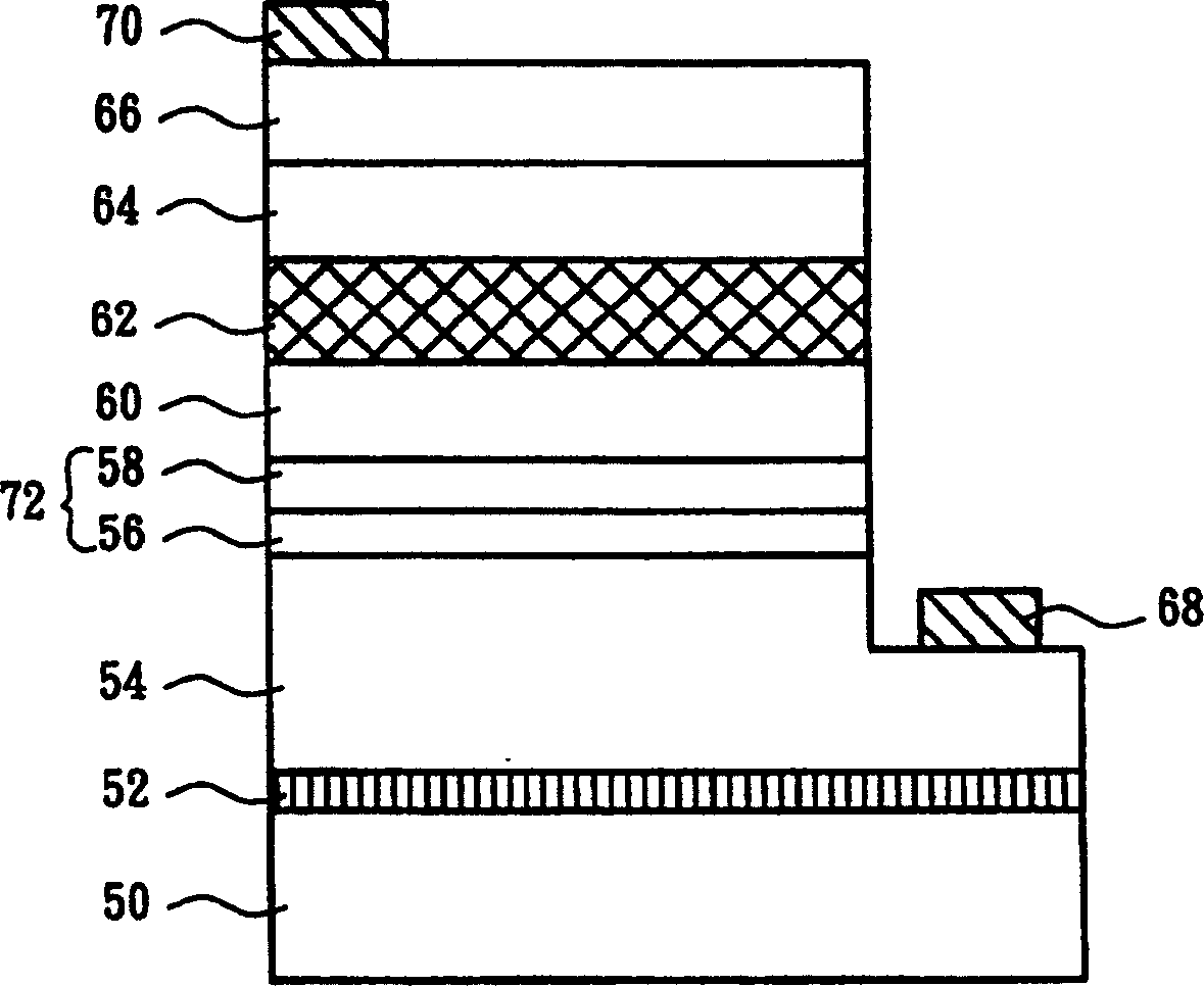
[0015] figure 2 It is a cross-sectional view of the structure of a III-nitride light-emitting diode according to the present invention. Please refer to figure 2 , the present invention uses a method for manufacturing a III-nitride light-emitting diode to simultaneously illustrate the structure of a III-nitride light-emitting diode. First, an epitaxial structure is formed on the substrate 50, and the epitaxial structure may sequentially include: a low-temperature buffer layer 52 (also known as a nucleation layer), an n-type ohmic contact layer 54, a degenerate junction (DegenerateJunction) 72, a wide energy gap p-type confinement layer 60 , active layer 62 , n-type confinement layer 64 with wide energy gap, and n-type ohmic contact layer 66 . Next, the n-type conductive electrode 68 and the conductive electrode 70 are vapor-deposited to complete the fabrication of the III-nitride light-emitting diode of the present invention. Among them, the III-nitride light-emitting diod...


PUM


Abstract

A degeneration interface layer is added between the active layer and the substrate in manufacturing III group nitride LED. The degeneration interface layer is composed of the n+ type layer and the p+type layer on the n+ type layer. Based on the degeneration interface layer, the III group nitride LED can be made in the form with n type in up and p-type in low and the conducting electrodes in LED are all n-types. The better current dispersibility provides by the n type nitride, which possesses higher adulterating concentration than the concentration the p-type possesses. Moreover, since the exposed part of the p-type nitride is reduced, it is not easy to affect the LED by the hydrogen passivation.

Description

(1) Technical field [0001] The invention relates to a nitride light-emitting diode, in particular to a nitride light-emitting diode with an upper n lower p form. (2) Background technology [0002] Light-emitting diodes are currently widely used in daily life, such as electronic signage, indicator lights and sensors. figure 1 What is shown is a cross-sectional view of the structure of an existing group III (in the periodic table of chemical elements) nitride light-emitting diode. Please refer to figure 1 , the general III-nitride light-emitting diode is in the form of upper p and lower n, that is, it is separated by the active layer 18, and the upper part is a p-type structure and the lower part is an n-type structure. The manufacturing method of III-nitride light-emitting diodes is as follows: a low-temperature buffer layer (buffer layer) 12, an n-type ohmic layer made of gallium nitride (GaN) are sequentially formed on a substrate 10 made of, for example, sapphire. A con...

Claims


Application Information

Patent Timeline
Patent Type & Authority Patents(China)
IPC IPC(8): H01L33/14
Inventor 汪信全陈锡铭
Owner EPISKY
Why Eureka
Try Eureka