
Vacuum field effect transistor

A vacuum field effect, transistor technology, used in vacuum tubes, transistors, discharge tubes, etc.

Inactive Publication Date: 2005-05-18
IKAIST CO LTD
View PDF0 Cites 2 Cited by
  • Summary
  • Abstract
  • Description
  • Claims
  • Application Information

AI Technical Summary

Problems solved by technology

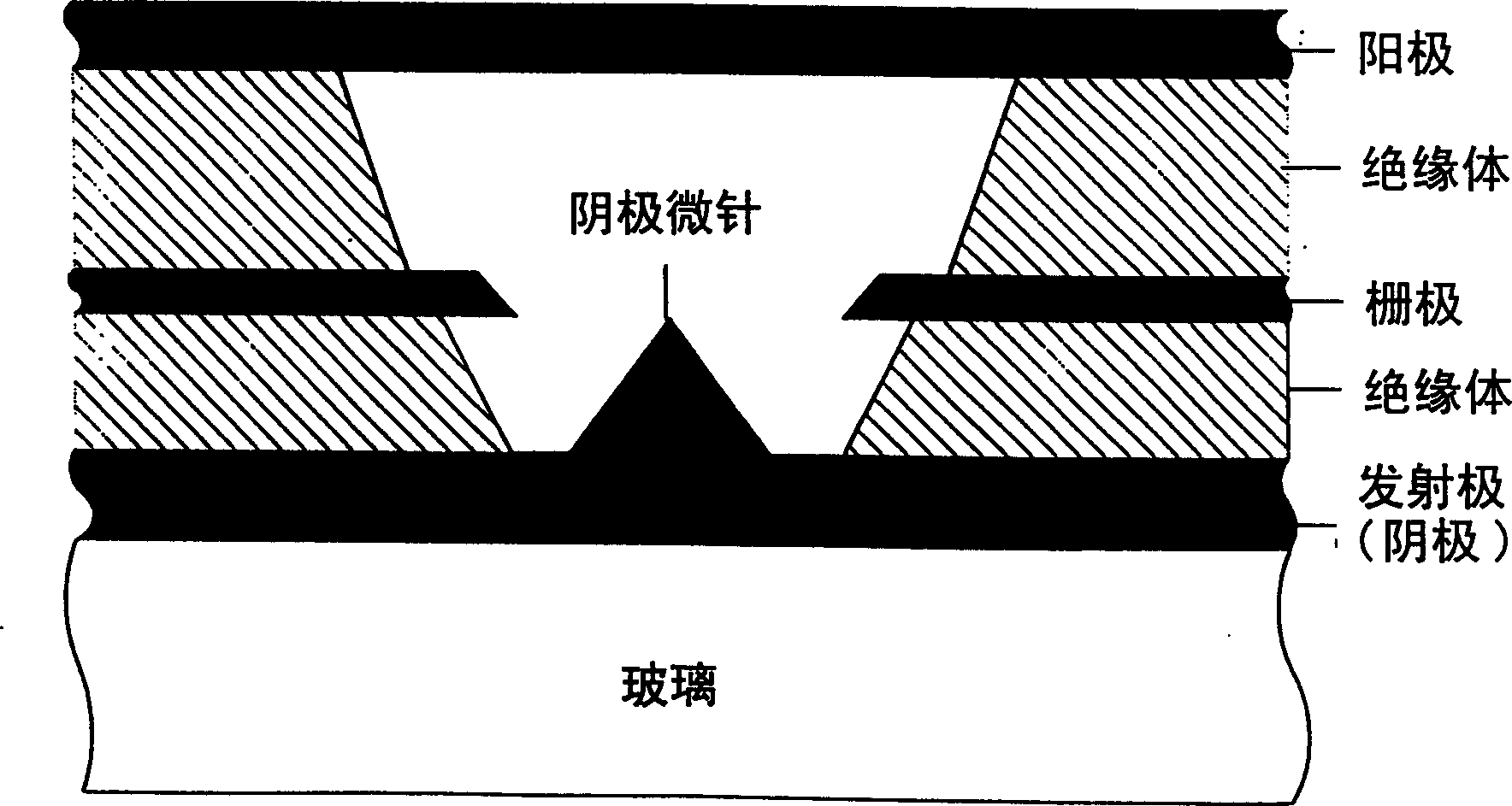
Together with the high anode-gate voltage, the difficulty of fabricating such microneedles limits the practical application of these vacuum transistor structures, such as military applications.

Method used


Image

  • Vacuum field effect transistor
  • Vacuum field effect transistor
  • Vacuum field effect transistor

Examples


Embodiment Construction

[0040] The preferred embodiments of the invention will be best understood by referring to the accompanying drawings, wherein like reference numerals are used for corresponding parts.

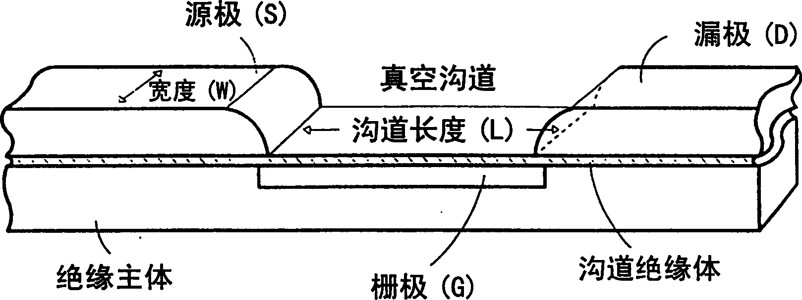
[0041] refer to Figure 3a with 3b, a structure is given, showing the basic concept of the VFT of the present invention in the form of a perspective view and a sectional view, respectively. This VFT structure seems to be a MOSFET structure, but the difference is that the channel is blanked and the gate is discharged in place. This VFT structure is divided into an upper structure consisting of a source S, a drain D and a vacuum channel therebetween, and a lower structure consisting of a gate G and a body. Each of the source S, the drain D and the gate G is a conductor, and an insulator with a vacuum channel between the upper structure and the lower structure. This vacuum channel is above the gate G, which is in an insulating body supporting the whole therebetween.

[0042] If a voltage is app...


PUM


Abstract

The invention discloses a planar / vertical vacuum field effect transistor (VFT) structure, which adopts a planar or vertical structure similar to a MOSFET to improve integration and can operate at a lower operating voltage at high speed. This planar type VFT includes source and drain electrodes made of conductors, which are kept on a thin channel insulator with a predetermined distance apart, with a vacuum channel in between; gate electrodes made of conductors, which have a certain The width is formed under the source and the drain, and the function of the channel insulator is to insulate the gate from the source and the drain; the insulating body is used as a substrate for supporting the channel insulator and the gate. A vertical vacuum field effect transistor comprising: a conductive continuous circular source having a vacant center formed on a trench insulator; a conductive continuous source formed under said trench insulator and extending across said source a gate; an insulating body serving as a substrate supporting the gate and a channel insulator; an insulating wall mounted above the source to form a closed vacuum channel; a drain formed above the vacuum channel . In both types an appropriate bias is applied between the gate, source and drain to enable electrons to be field emitted from the source to the drain through the vacuum channel.

Description

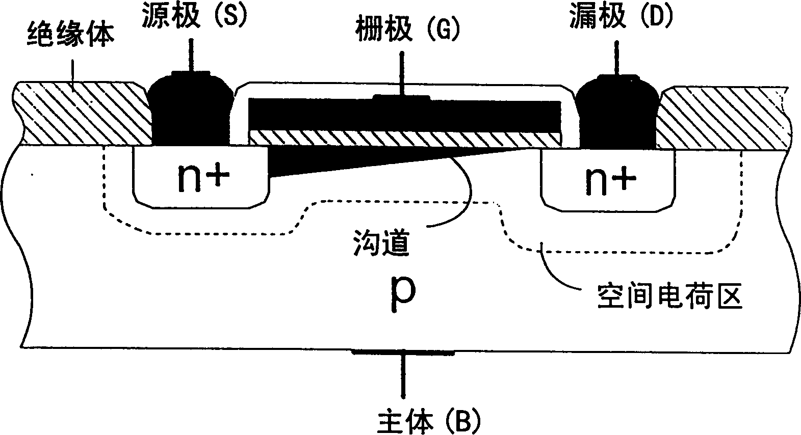
technical field [0001] The present invention relates to a planar / vertical vacuum tunnel transistor. Specifically, the present invention relates to a planar / vertical vacuum tunnel transistor, which adopts a planar or vertical structure of a MOSFET to improve integration and operate at a lower operating voltage at high speed. Background technique [0002] In ordinary semiconductor devices, current conducts in the semiconductor, causing the movement speed of electrons to be affected by the crystal lattice or impurities in it. Recently, semiconductor devices including microneedle type vacuum transistors have been developed. In this type of transistor, electrons move in a vacuum, so the speed is not limited. Thus, such transistors can operate at extremely high speeds. However, their disadvantages are that they are difficult to integrate on a large scale and require high operating voltages. [0003] In order to better understand the background art of the present invention, a d...

Claims


Application Information

Patent Timeline
Patent Type & Authority Patents(China)
IPC IPC(8): H01L29/66H01J1/316H01J19/24H01J19/32H01J21/10H01L29/78H01L29/786
CPCH01J1/316H01J21/105
Inventor 曹圭亨柳之烈黄明运赵敏衡禹永振金荣基
Owner IKAIST CO LTD
Learn More