
Process for forming transistor with metallic silicide on source and drain

A technology of metal silicide and metal silicide layer, which is used in semiconductor/solid-state device manufacturing, electrical components, circuits, etc., and can solve the problems of low energy use efficiency, low efficiency, and difficult to form accurately.

Inactive Publication Date: 2005-03-30
VANGUARD INTERNATIONAL SEMICONDUCTOR CORPORATION
View PDF0 Cites 0 Cited by
  • Summary
  • Abstract
  • Description
  • Claims
  • Application Information

AI Technical Summary

Problems solved by technology

Since metals are generally formed by physical vapor deposition (physical vapor deposition, PCD) (sputtering, evaporation) or chemical vapor deposition (chemical vapor deposition; CVD), and evaporation is not easy to control the composition of the evaporated metal and form a step coverage For metals with good properties, the energy usage efficiency of sputtering is not high and the step coverage of the formed metal is not good, and chemical vapor deposition is difficult to avoid the problems of by-products and pollution as mentioned above
Obviously, this approach is not efficient and does not form the exact desired metal

Method used


Image

  • Process for forming transistor with metallic silicide on source and drain
  • Process for forming transistor with metallic silicide on source and drain
  • Process for forming transistor with metallic silicide on source and drain

Examples


Embodiment Construction

[0022] A preferred embodiment of the present invention is a method of forming a metal-oxide-semiconductor transistor with metal silicide on the source and drain, comprising at least the following steps:

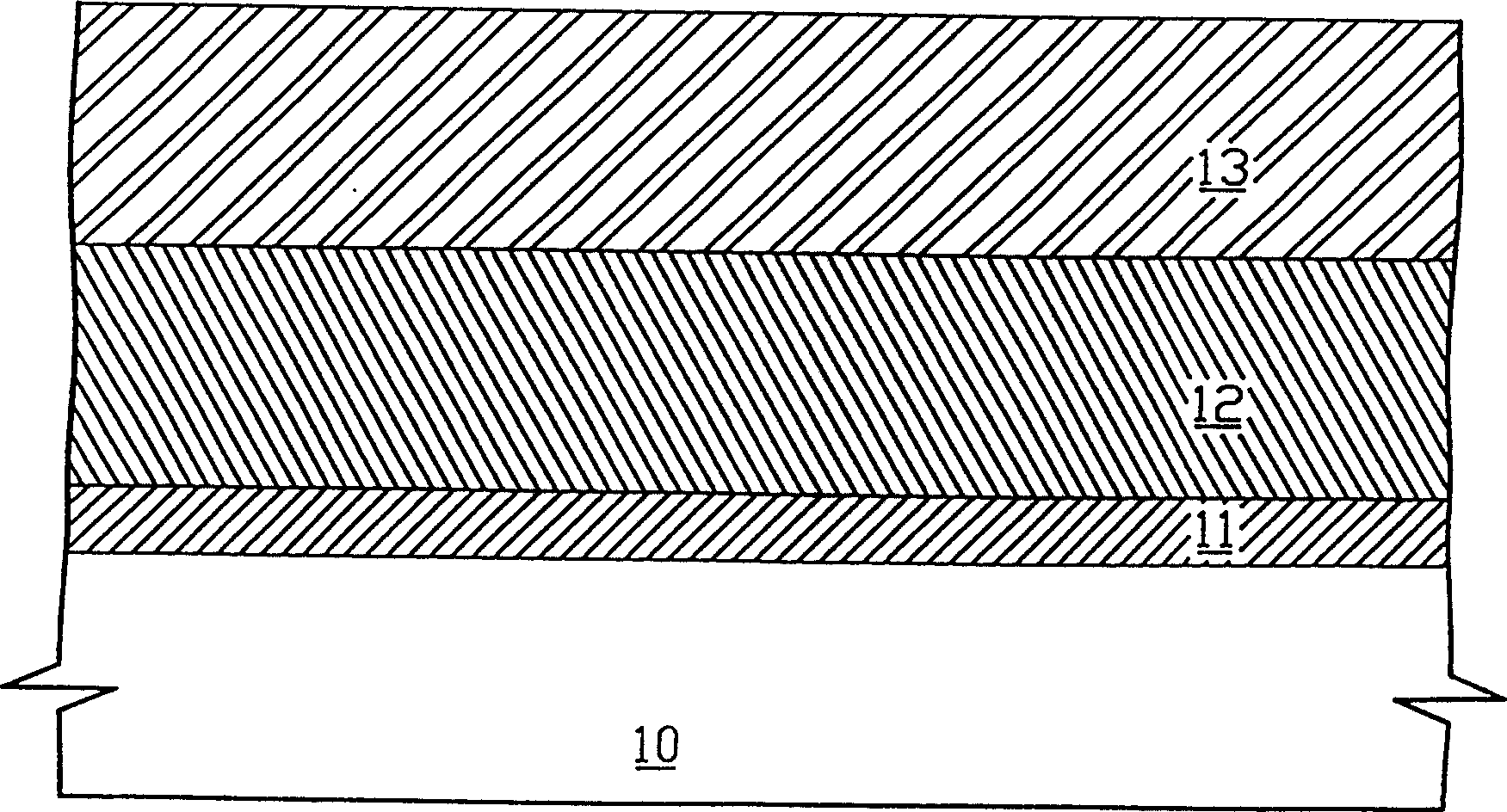
[0023] like Figure 1A As shown, a silicon substrate 10 is provided and a first dielectric layer 11 is formed on the silicon substrate 10. Here, the first dielectric layer 11 can at least serve as a gate dielectric layer. The first dielectric layer 11 is typically an oxide layer, and typically has a thickness of about 50 to 300 angstroms.

[0024] like Figure 1B As shown, a conductor layer 12 is formed on the first dielectric layer 11 and a second dielectric layer 13 is formed on the conductor layer 12 . The conductor layer 12 can be used at least as a gate conductor layer. The conductor layer 12 can be one of the following: a metal layer, a polysilicon layer and a polysilicon metal layer, and its typical thickness is about 500 angstroms to 3500 angstroms. The second diel...


PUM

PropertyMeasurementUnit
Thicknessaaaaaaaaaa
Thicknessaaaaaaaaaa
Thicknessaaaaaaaaaa

Abstract

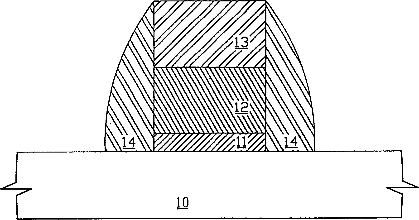
The invention relates to a method for manufacturing MOS transistor with metal silicide on source and drain. The technical steps are as follows: First dielectric substance layer, conductor layer, second dielectric substance layer are formed on silicon substrate. Eliminating part of the second dielectric substance layer and part of the conductor layer in procedure of transferring pattern forms a grid structure. Gap wall is formed on side wall of the grid structure. Metal granule is adulterated to silicon substrate, where the granule can penetrate through first dielectric substance layer to the silicon substrate, but can not penetrate through the second dielectric substance layer to the conductor layer. Heat-treatment step is carried on to form metal silicide layer on the silicon substrate and eliminate the non-reacted part of metal granule.

Description

technical field [0001] The present invention relates to a method of forming a metal oxide semiconductor transistor, in particular to a method of forming a metal oxide semiconductor transistor which can reduce side effects and control the position of metal silicide. Background technique [0002] Due to the advantages of low resistance, high temperature resistance, and easy integration with polysilicon, metal silicides have been widely used in the manufacturing process of semiconductor devices, such as for connecting metal interconnects to the source and drain of transistors. Part of the pole or part of the polycide used as the gate. [0003] There are two methods for forming metal silicide in the prior art: one is to form a metal silicide layer directly on the substrate; the other is to form metal on the substrate first, and then use a heat treatment process to make the metal react with silicon And generate metal silicide. [0004] The former method reacts a silicon-contain...

Claims


Application Information

Patent Timeline
IPC IPC(8): H01L21/283H01L21/314H01L21/3205H01L21/336
Inventor 曾鸿辉
Owner VANGUARD INTERNATIONAL SEMICONDUCTOR CORPORATION
Learn More