
Patsnap Eureka
For R&D, Patsnap Eureka makes reading and utilizing patents & technical documents easy.
Patsnap Eureka AIR
Designed for self-driven R&D workflows. Generate viable solutions, solve complex R&D challenges, empower your innovation with AI.

Patsnap Eureka Materials
Designed for material experts only. Revolutionize your material R&D, from search, analyze, to developing new materials.

TechResearch
Generate reliable direction feasibility study reports for your R&D in just a few steps.

TechSeek
Discover and master advanced knowledge NOW. Basics, ideas, possibilities, all at once.

TechMind
As an expert in R&D Theories, TechMind can generates customized viable solutions instantly.

TechRisk
Analyze your overall solution with one click, know your potential R&D risks in advance.

TechMonitor
Get weekly tech updates, stay abreast of the latest tech innovations and key insights.
Composite adhesive film production process and application thereof in fingerprint chip packaging field
A production process and technology for fingerprint chips, applied in film/sheet release liners, adhesives, film/sheet adhesives, etc., can solve the problems of wrinkled chip sidewalls, easy pollution of the surrounding environment, whitening, etc. , to achieve the effect of improving hardness and wear resistance, improving batch stability, and facilitating molding
- Summary
- Abstract
- Description
- Claims
- Application Information
AI Technical Summary
Problems solved by technology
Method used
Image

Examples
specific Embodiment approach 1
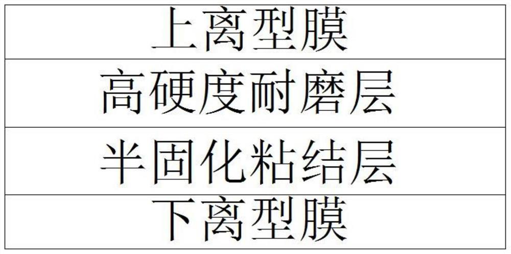
[0028] For the first specific implementation, please refer to Figure 1-2 , the present invention provides a technical solution: a composite film production process, including making a high-hardness wear-resistant layer, making a semi-cured adhesive layer and a composite upper and lower layer: using a precision coating machine, first coat the upper release film. High-hardness wear-resistant layer with cloth thickness of 10-25μm; coat semi-cured adhesive layer of 15-40μm thickness on the lower release film; use hot composite rollers to continuously apply the upper release film, high-hardness wear-resistant layer, semi-cured The adhesive layer and the lower release film are combined to form a roll-shaped integrated film;
[0029] The upper release film in step 1 is a mirror-surface release film, and after the adhesive film is cured, the appearance effect of a mirror surface is obtained; the lower release film in step 1 is a matte frosted release film, and the matte frosted relea...
Embodiment 1
[0035] First: select ELD type PET film with a thickness of 50 μm, ELD type PET film transmittance > 90%, haze value < 5%, apply non-silicon release agent on the film and obtain the upper release film; use Slot extrusion coating machine, coat a high-hardness wear-resistant layer with a thickness of 10-25 μm on the non-silicon release agent surface of the upper release film, use the coating machine oven to dry the solvent, and roll the material.
[0036] Secondly: apply a semi-cured adhesive layer with a thickness of 15-40μm on the release surface of the lower release film, preferably a coating thickness of 30±1μm; for the convenience of distinction, the choice of the lower release film is generally different from the color of the upper release film .
[0037] Then: use a heated composite roller to roll the high-hardness wear-resistant layer and the semi-cured adhesive layer together, and then roll the material.
[0038] Then: Die the roll film into a suitable size from the rol...
Embodiment 2
[0043] First: choose YGD type PET film with a thickness of 50 μm, the film haze value of YGD type is less than 65%, matt and matt, and apply non-silicon release agent on the film to obtain an upper release film. Then coat the release film with a slit extrusion coater, coat a high hardness wear-resistant layer with a thickness of 10-25 μm on the non-silicon release agent surface of the upper release film, and bake it with a coater oven. Dry solvent, rewinding in roll form, preferably coating thickness 25±1μm.
[0044] Secondly: apply a semi-cured adhesive layer with a thickness of 15-40μm on the release surface of the lower release film, preferably a coating thickness of 30±1μm; for the convenience of distinction, the choice of the lower release film is generally different from the color of the upper release film .
[0045] Then: use the heated composite roller to roll the high hardness wear-resistant layer and the semi-cured adhesive layer together, and then roll the material...
PUM
 Abstract
Description
Claims
Application Information
 - R&D Engineer
- R&D Manager
- IP Professional
- Industry Leading Data Capabilities
- Powerful AI technology
- Patent DNA Extraction
Browse by: Latest US Patents, China's latest patents, Technical Efficacy Thesaurus, Application Domain, Technology Topic, Popular Technical Reports.
© 2024 PatSnap. All rights reserved.Legal|Privacy policy|Modern Slavery Act Transparency Statement|Sitemap|About US| Contact US: help@patsnap.com