Preparation method of GaN Schottky diode and GaN Schottky diode
A Schottky diode and electrode layer technology, which is applied in semiconductor/solid-state device manufacturing, semiconductor/solid-state device parts, semiconductor devices, etc., can solve the problems of long cycle, high cost of terminal structure, complex process, etc., and reduce the peak value Electric field, reduced production cost, simple preparation method
- Summary
- Abstract
- Description
- Claims
- Application Information
AI Technical Summary
Problems solved by technology
Method used
Image

Examples
Embodiment 1
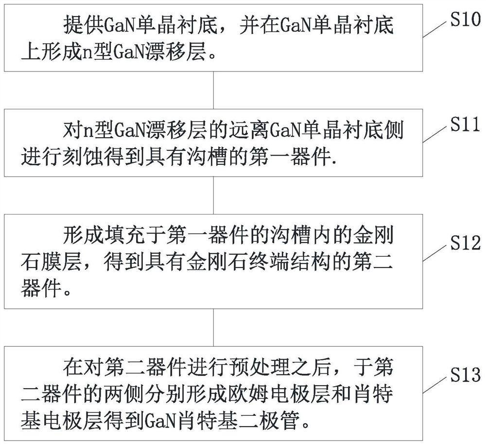
[0044] see figure 1 , in this embodiment, a preparation method of a GaN Schottky diode, comprising:
[0045] In step S10 , a GaN single crystal substrate 1 is provided, and an n-type GaN drift layer 2 is formed on the GaN single crystal substrate 1 .
[0046] Step S11, etch the side of the n-type GaN drift layer 2 away from the GaN single crystal substrate 1 to obtain a first device (such as Figure 4 shown).
[0047] Step S12, forming the diamond film layer 5 filled in the groove 21 of the first device to obtain a second device (such as a diamond terminal structure) Figure 5 shown).
[0048] Step S13, after preprocessing the second device, respectively forming an ohmic electrode layer 4 and a Schottky electrode layer 3 on both sides of the second device to obtain a GaN Schottky diode (such as Image 6 shown).
[0049] Specifically, a plurality of trenches 21 can be provided, and each trench 21 is provided at intervals; the Schottky electrode layer 3 covers part of the o...
Embodiment 2
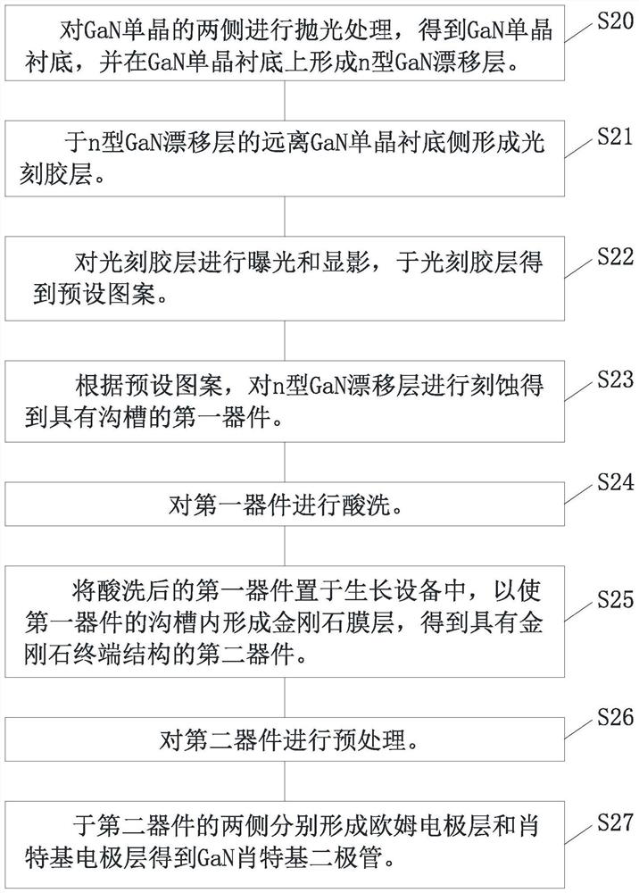
[0051] see figure 2 Step S20 , polishing both sides of the GaN single crystal to obtain a GaN single crystal substrate 1 , and forming an n-type GaN drift layer 2 on the GaN single crystal substrate 1 .
[0052]Specifically, the two opposite sides of the GaN single crystal are ground and polished to obtain a GaN single crystal with two smooth sides, so that the subsequent GaN single crystal substrate 1 and the Schottky electrode layer 3 and the GaN single crystal substrate 1 and n The bonding between the GaN drift layers 2 is tighter, thereby improving the stability of current transfer in the GaN Schottky diode. The carrier concentration of the GaN single crystal substrate 1 is greater than 1E18cm-3, preferably 2E18cm-3, to ensure that the GaN single crystal substrate 1 has good electrical conductivity; the thickness of the GaN single crystal substrate 1 ranges from 150um- 400um, preferably 300um, so that the GaN single crystal substrate 1 can provide sufficient support stre...
Embodiment 3
[0085] see Figure 4 , Figure 5 as well as Image 6 , in this embodiment, a GaN Schottky diode, made by the above-mentioned preparation method of a GaN Schottky diode, includes a GaN single crystal substrate 1, which is stacked on one side of the GaN single crystal substrate 1 The n-type GaN drift layer 2 and the Schottky electrode layer 3, and the ohmic electrode layer 4 stacked on the other side of the GaN single crystal substrate 1, the side of the n-type GaN drift layer 2 away from the GaN single crystal substrate 1 There is a trench 21, the trench 21 is filled with a diamond film layer 5, the diamond film layer 5 forms a diamond termination structure in the n-type GaN drift layer 2, and the Schottky electrode layer 3 covers a part of the opening of the trench 21.
[0086] Specifically, two trenches 21 are provided, and the two trenches 21 are respectively provided at both ends of the n-type GaN drift layer 2 . The trenches 21 are rectangular, and the depth of the trenc...
PUM
| Property | Measurement | Unit |
|---|---|---|
| thickness | aaaaa | aaaaa |
| thickness | aaaaa | aaaaa |
| thickness | aaaaa | aaaaa |
Abstract
Description
Claims
Application Information
 - R&D
- Intellectual Property
- Life Sciences
- Materials
- Tech Scout
- Unparalleled Data Quality
- Higher Quality Content
- 60% Fewer Hallucinations
Browse by: Latest US Patents, China's latest patents, Technical Efficacy Thesaurus, Application Domain, Technology Topic, Popular Technical Reports.
© 2025 PatSnap. All rights reserved.Legal|Privacy policy|Modern Slavery Act Transparency Statement|Sitemap|About US| Contact US: help@patsnap.com