Circuit-embedded PCB manufacturing method and circuit-embedded PCB

A manufacturing method and circuit technology, applied in the directions of multilayer circuit manufacturing, final product manufacturing, sustainable manufacturing/processing, etc., can solve problems such as PCB tolerance and increased surface roughness of circuits, so as to avoid increased surface roughness and improve manufacturing Effect of precision, tolerance avoidance

Pending Publication Date: 2022-08-02
DONGGUAN SHENGYI ELECTRONICS
View PDF0 Cites 0 Cited by
  • Summary
  • Abstract
  • Description
  • Claims
  • Application Information

AI Technical Summary

Problems solved by technology

[0005] The object of the present invention is to provide a PCB manufacturing method for buried circuits and a PCB for buried circuits, which can solve the problem of tolerances in the circuit etching process of existing PCBs, and avoid the problems caused by the browning treatment of the circuits. The problem of increasing the surface roughness of the circuit, so as to ensure that the insertion loss performance of the PCB meets the signal transmission requirements

Method used


Image

  • Circuit-embedded PCB manufacturing method and circuit-embedded PCB
  • Circuit-embedded PCB manufacturing method and circuit-embedded PCB
  • Circuit-embedded PCB manufacturing method and circuit-embedded PCB

Examples


Embodiment Construction

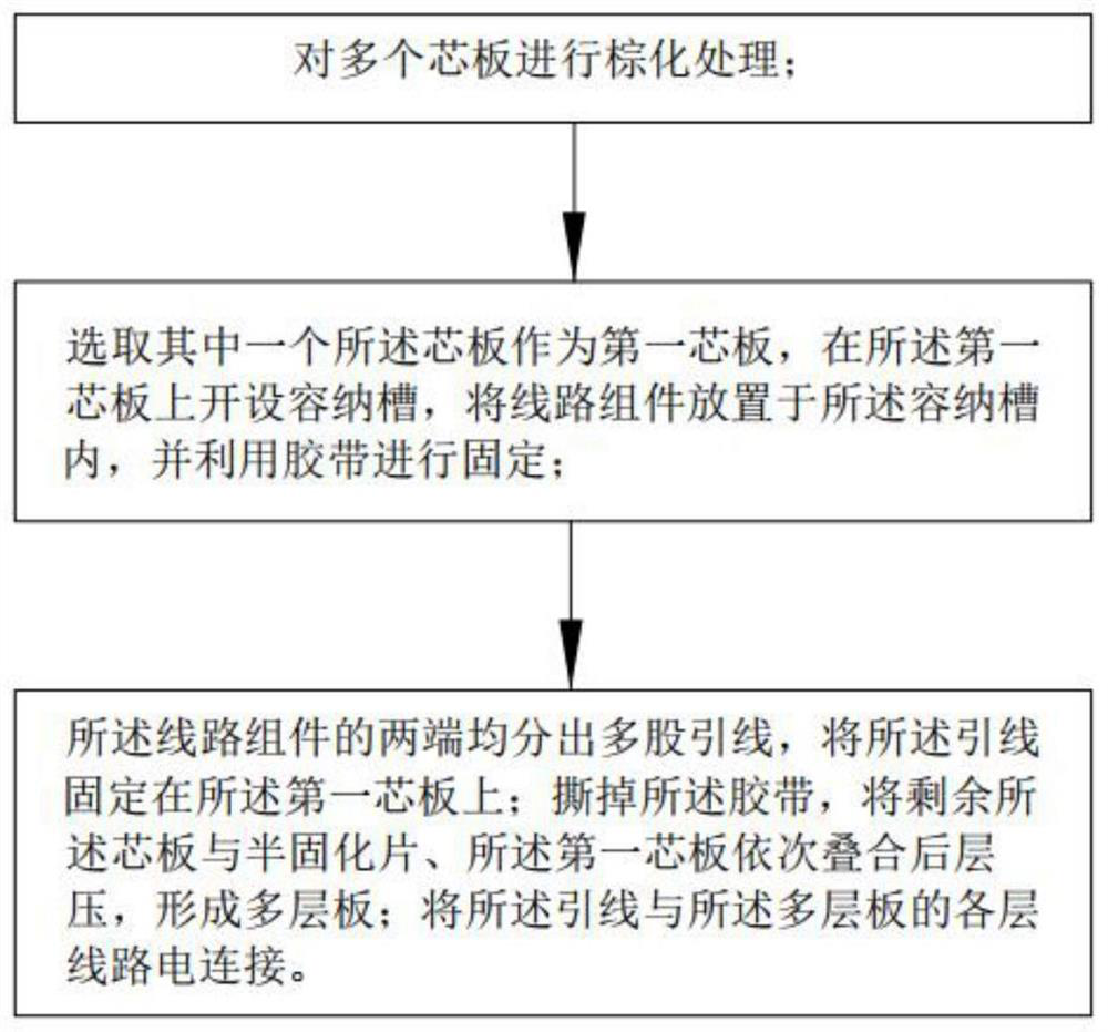
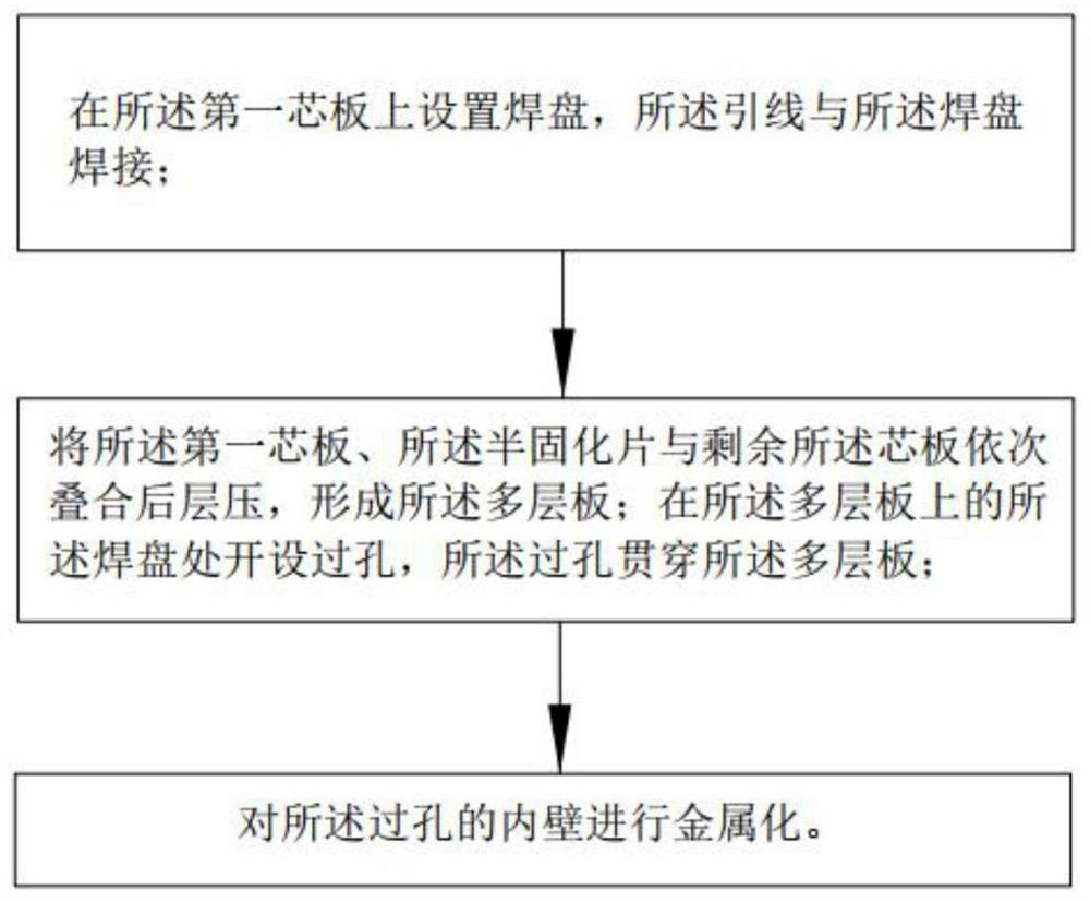
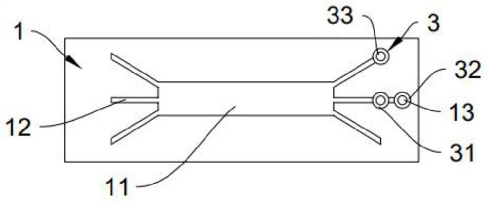
[0045] In order to make the purposes, technical solutions and advantages of the embodiments of the present invention clearer, the technical solutions in the embodiments of the present invention will be clearly and completely described below with reference to the accompanying drawings in the embodiments of the present invention. Obviously, the described embodiments These are some embodiments of the present invention, but not all embodiments. The components of the embodiments of the invention generally described and illustrated in the drawings herein may be arranged and designed in a variety of different configurations.

[0046] Thus, the following detailed description of the embodiments of the invention provided in the accompanying drawings is not intended to limit the scope of the invention as claimed, but is merely representative of selected embodiments of the invention. Based on the embodiments of the present invention, all other embodiments obtained by those of ordinary ski...


PUM


Abstract

The invention discloses a circuit-embedded PCB manufacturing method and a circuit-embedded PCB, and relates to the technical field of circuit board manufacturing. According to the manufacturing method of the PCB with the embedded circuit, the circuit assembly serves as an independent unit, the containing groove is formed in the first core board subjected to brownification treatment, and then the containing groove and the adhesive tape are used for fixing the circuit assembly, so that the circuit assembly is prevented from deviating during lamination, and the manufacturing precision of the PCB is improved. Finally, the leads are electrically connected with all layers of circuits of the multilayer board, so that the circuit assembly is electrically connected with all layers of circuits, the PCB with the embedded circuits is generated, the problem that machining tolerance occurs in the circuit etching machining process of an existing PCB is solved, the problem that the surface roughness of the circuits is increased due to the fact that the circuit assembly is subjected to browning treatment is solved, and the production efficiency is improved. Therefore, the insertion loss performance of the PCB is ensured to meet the signal transmission requirement.

Description

technical field [0001] The invention relates to the technical field of circuit board fabrication, in particular to a PCB fabrication method with embedded circuits and a PCB with embedded circuits. Background technique [0002] In recent years, with the continuous development of electronic products, higher requirements have been placed on the integrity of signal transmission. The more complete the signal transmission, the smaller the loss of the signal during the transmission process. Therefore, the insertion loss performance of the PCB (Printed Circuit Board, printed circuit board) is very important to whether the PCB meets the signal transmission requirements. [0003] The circuit of the existing PCB is mainly fabricated by circuit etching on the metal layer, so as to realize the circuit production of the PCB. However, in the process of PCB production in the traditional way, in order to improve the bonding force of the lamination process, it is necessary to carry out brown...

Claims


Application Information

Patent Timeline
IPC IPC(8): H05K3/46
CPCH05K3/4614Y02P70/50
Inventor 何醒荣王小平杨凡董凤蕊林桂氽
Owner DONGGUAN SHENGYI ELECTRONICS
Why Eureka
Try Eureka